The basic element in a computer can be an electromagnetic relay, a vacuum tube, or a transistor. All three of these can function as switches which are electrically controlled. Of course, vacuum tubes and transistors can also function as analogue amplifiers, producing an output which is an amplified replica of the input; they don't need to be simply either "off" or "on". This means that a computer can use small and cheap vacuum tubes or transistors; while its components need to be reliable, they don't need to be high-quality in all respects. One transistor logic family, ECL (emitter-coupled logic), used in many of the highest-speed computers, takes advantage of the fact that a transistor can respond more quickly to its input if it does not have to go all the way from a fully-on state to a fully-off state.
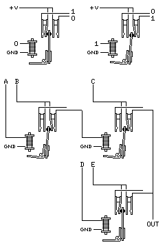
With relays, it is simple to understand how basic logic functions, such as AND, OR, and NOT, can be implemented:
In the top of the diagram, we see a single relay in both its OFF and ON states. When no current is flowing through the magnet, the armature is at rest, so the switch on the left, near the coil, is closed, while the switch on the right, away from the coil, is open. If one connection to each switch is connected to the power, then the other connection on the first switch provides a signal that is the opposite of that going into the magnet, and the other connection on the second switch provides a signal that is the same as that going into the magnet. This shows how a relay can be used as an inverter.
In the bottom of the diagram, we see how the AND and OR functions are achieved with relays. For current to flow out of a switch, the switch needs to be on, and the other end of the switch has to be connected to a possible source of current. So the signals A and B both must be live for the first relay in the diagram to produce a signal, and the second relay applies the signal labelled C as well, to produce a three-input AND gate. The third relay on the botton produces the AND of D and E. As signals are either live and positive, or disconnected (and thus in what is known as a "high impedance" state) the outputs of the second and third relays simply need to be joined together to perform the OR operation.
Electronic logic, involving vacuum tubes or transistors is not quite as simple and convenient as relay logic, but the basic logical functions can still all be produced.
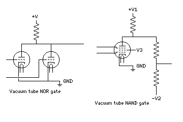
This diagram shows two types of gates that can be made from vacuum tubes. The first is a triode NOR gate, the second a pentode NAND gate. The pentode NAND gate needs a level translation circuit so that its output has the same voltage levels as its inputs, and its power supplies are at significantly different voltages from its logic levels.
The diagram below:
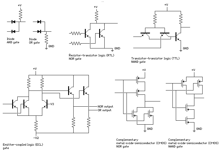
shows a few familes of solid-state logic.
Note that the gates have been named with the assumption that a positive voltage represents 1 and a negative voltage represents 0. This is merely a convention. In a logic family where the NOR gate is the basic construct, since AND gates are more common than OR gates in most digital circuits, the convention can be reversed so that the NOR gate becomes a NAND gate.
The AND and OR gates shown for diode logic are not complete in themselves; in addition to the fact that an inverter cannot be made without amplifying components, the lack of amplification limits the complexity of logic circuits that can be built with them.
But computers have been built using primarily diode logic, and the occasional vacuum tube for amplification; and a gate design involving diode logic governing the input to a transistor is the core of the logic family diode-transistor logic (DTL), not shown in the diagram.
Both RTL and DTL had some significant limitations that TTL overcame, making it the most popular bipolar logic family. ECL, because it made use of a switch between smaller signal levels, did not require waiting for transistors to go into saturation; while it was elaborate, and consumed more current, it was therefore used when the very highest performance was desired.
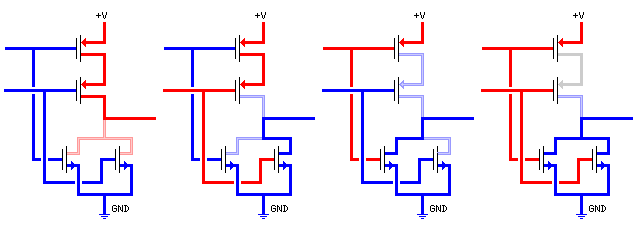
Only one logic family using MOSFET transistors is illustrated, CMOS. In CMOS, every logic gate is implemented twice, once as itself in positive logic, and once as its opposite in negative logic. Although this seems wasteful, it has important advantages.
A CMOS gate connects its output either to the positive supply or to ground. It doesn't contain any resistors, so it doesn't produce voltages that are produced by the continuous flow of current through a resistor.
Relay logic also had this desirable characteristic; but power was still constantly consumed, through the coil of the relay's electromagnet, whenever the relay was on. The input of a transistor is itself of high impedance, so it only demands that a small trickle of current flow into it.
This very low power consumption made the extremely high packing density of current integrated circuits feasible.
It is not entirely without disadvantages. Bipolar transistors come in two kinds, PNP and NPN. And, similarly, there are two kinds of field-effect transistors, p-channel and n-channel. The NPN and the n-channel transistor are generally preferred for higher quality circuits (thus, NMOS was used for microprocessors while PMOS was used for calculator chips); metals conduct using electrons and not holes, and, thus, it is easier for low resistivities to be achieved in semiconductors doped with a donor impurity. A CMOS gate requires both kinds of MOSFET, and is thus limited by the characteristics of its p-channel MOSFETs.
The diagram below shows, on the left, how CMOS circuitry is often constructed in practice: instead of using separate CMOS NAND and NOR gates, more complex circuits combining AND and OR functions are built up, along with their mirror images, on each side of a compound gate.
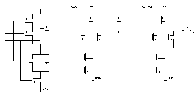
The middle of the diagram illustrates what is known as domino logic. This addresses the problem that the p-channel MOSFETS limit the performance of a CMOS gate by building the logic circuit out of n-channel MOSFETS only, using only one p-channel MOSFET, along with a corresponding n-channel MOSFET for a clock signal. The result of doing this, called dynamic CMOS, is a circuit whose output can drive regular CMOS circuitry, but not another dynamic CMOS circuit; the addition of a CMOS inverter on the output, as shown, leads to domino logic. In practice, the logic circuit built from n-channel MOSFETS would be more complex than the three-gate example shown here.
On the right side of the diagram, we see the gate design used in the CELL microprocessor, jointly designed by IBM and SONY. In this pseudo-NMOS design, the two clock phases are non-overlapping, preventing waste due to current flowing through both of the clock transistors, as they are never both on at the same time.
A capacitor, implemented, as usual for integrated circuits, by a reverse-biased diode, is applied to the output of the gate.
The diagram below illustrates how a CMOS NOR gate works for the different possible inputs it may receive:
Areas at a positive potential are shown in red, those at a negative potential are shown in blue. By-ways, down which very little current, and that incidental to the operation of the device, would flow are shown in a lighter color. Note that the path between the two series transistors in the case of two positive inputs to the device is shown as gray, as it is isolated by two non-conducting transistors from both the positive and negative supplies.
Current flows to the output from the positive supply at the top when a negative input makes both of the p-channel MOSFETs in series at the top conduct; current flows from the output into the ground at the bottom when a positive input makes either of the n-channel MOSFETs in parallel at the bottom conduct.
Note that one way current can be consumed in CMOS is when, during switching, for a brief moment both the top and bottom parts conduct, if one pair of transistors receives signals before the other pair.
Also note that the other transistor logic families did not attempt to obtain an AND logic function by placing transistors in series; this generally means that the input voltages to the transistors would differ, one being closer to the positive supply than the other, and that the voltage across the transistor would differ.
Here is a diagram of how a CMOS NOR gate, such as the one described above, might look on an integrated circuit chip fabricated in an n-well process:
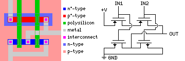
Note the key to the various areas on the chip, and the schematic at the right which attempts to illustrate the location of the transistors in the actual form of the gate.
More information on how modern CMOS chips are designed and made is available here.
CMOS was first described in a paper published in 1963; a patent for it, U.S. Patent 3,356,858, was not issued until 1967, to one of the paper's authors, F. M. Wanlass, and assigned to his employer, Fairchild.
A bipolar logic family once thought very promising that also dispenses with resistors is Integrated Injection Logic.
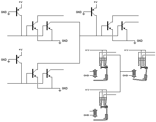
In I2L, the fundamental unit is not the AND or OR gate; logic is accomplished by a wired-OR function. But inverters with multiple outputs are needed, so that multiple OR combinations involving one common signal are kept separate. A wired-OR between three two-output inverters is shown in the diagram above, and the equivalent construct using relays as logic elements is shown in the lower right of the diagram.
While there are no actual resistors in I2L logic, the PNP transistor whose emitter is connected to +V in the two-output inverters shown above has a function similar to that of a resistor. But because it is a transistor, it responds to the voltage level connected to its collector, leading to similar economies of energy to those of CMOS, if not quite as close to perfection.
Closely related to ECL, a little-known early high-speed logic family was CTL, or complementary transistor logic. Fairchild was one of the main companies producing ICs belonging to this family. (Interestingly enough, they currently make microchips with a trademarked technology called Current Transfer Logic, this being a completely different, low-power and low-noise technology, but having the same initials.) It is of some historical importance; this is the logic family used in the NEAC 2200/500, produced by NEC, which was the first Japanese computer to use only ICs, and no discrete transistors, for its logic, and, closer to home, it was the logic family used in the IC-6000 by Standard Computer, which was a microprogrammable computer, available in 1966, which could either emulate the IBM 7090 family of computers, or use a custom instruction set for enhanced FORTRAN performance. As well, it was used in the Hewlett-Packard 3000, and some Burroughs machines.
The following illustration of a CTL gate:
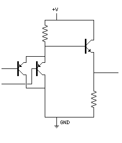
was only possible thanks to this site, which seems to be the only place where this logic family is still described on the Web! The site notes that, since like ECL, it is a design based on analogue amplification, obtaining speed by avoiding saturating the transistors, noise can propagate through the design.
Although this looks like the part of the ECL gate that performed a NOR logic function, since the two input transistors have been reversed, this is an AND gate, since it is now a low input voltage rather than a high one which would make these transistors conduct.
Since I wrote this, I was able to find more information about this logic family through a 1969 Fairchild catalogue. This logic family is actually referred to as Complementary Transistor Micrologic there, and perhaps one of its most serious limitations was that in addition to ground and +4.5 volts, a power supply of -2 volts was also required by it.
For further confusion, the term Complementary Transistor Logic is sometimes also used to describe a logic family strictly analogous to CMOS, but using bipolar transistors (unlike Integrated Injection Logic, which we've seen is significantly different from CMOS in principle, despite having some similarities in the benefits which it promised).
IBM worked on an improved version of this kind of logic, called Current Buffered Logic. The reason this never achieved commercial use, despite seeming like an obvious idea, is that the kinds of transistors required to make it work at desirable speeds would require too complex an IC fabrication process. Of course, it is entirely possible that in some materials other than silicon, where fabricating reasonably good bipolar transistors of both kinds, NPN and PNP, is easier than fabricating reasonably good p-channel and n-channel MOS transistors, this might end up being preferred to CMOS.
There are many other possible logic families. For example, in the IBM System/390 computer, a logic family called DCS was used. A DCS gate appears almost identical to an ECL gate, except that the complement of an input bit goes to the other arm of the differential amplifier instead of simply having only one transistor there with a reference voltage.
The following diagram illustrates the arrangement of a core plane:
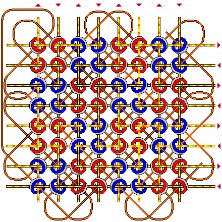
The wires running vertically and horizontally through the ferrite rings are the drive wires. The current going through each wire is carefully chosen, in relation to the magnetic characteristics of the cores, so that if a current flows through one of the drive wires passing through a core, nothing will happen, but if a current flows through both of the drive wires that pass through the core, the core will become magnetized in the direction determined by those currents. One of the results of the need to choose the current used carefully was that many core memory arrays either had their temperature controlled, or their temperature was measured, and circuitry was used to adjust the currents used to correspond with their current operating temperature.
The vector sum of the two currents will follow the same diagonal direction as the other wire shown passing through each core, the sense wire, and thus the magnetization will be along the circumference of the ferrite ring, in either a clockwise or a counter-clockwise direction.
If a core is being magnetized in the same direction in which it is already magnetized, not much will happen, but if it is magnetized in the opposite direction, a faint electrical pulse will be detected along the sense wire.
Hence, one reads a bit from a core plane by storing a zero in that bit; then, after one has read the bit that was there, one can go back and write the old value back in again.
Normally, of course, a whole computer word is read from a core memory at once, and so several core planes in parallel are read or written; thus, there is no opportunity to skip the write-back step if a zero is read.
Also, it is important that the two currents from the drive lines flow through the core in the same direction; whether the pulse on the sense line is positive or negative is not important, since the amplifier for that line can be designed to produce a logic signal in either case.
Thus, the annular faces of the ferrite cores have been colored either red or blue in the diagram; inspection of the diagram will show that on any drive line, horizontal or vertical, a red face is always directed in the opposite direction, with respect to that drive line's direction, to that in which a blue face is directed.
Note also that the ferrite rings have been tilted back, so that one of their faces is visible, and they could have been tilted back in either of two directions in each case. The pattern chosen in this diagram was one which has, as a result, the property that the cores oriented along each of the two diagonal axes of the diagram alternate in the direction they are tilted as the sense line alternates in the direction in which it passes through them; thus, the color of the face of the core indicates the polarity of the pulse it will send on the sense line.
As long as both the vertical and horizontal drive lines alternate from one line to the next in the direction current travels through them, if the two drive lines passing through one core work in the same direction, they will all work in the same direction.
The type of core memory illustrated above was known as 2 1/2 dimension core memory. A core in the type of core plane shown above is selected when both the X and Y lines going through that core have a pulse sent through them. When several core planes contain the individual bits of a word in memory, this means that for either the X lines or the Y lines, at least, separate drive circuits are needed for each plane.
This was avoided in standard 3-D core memory:
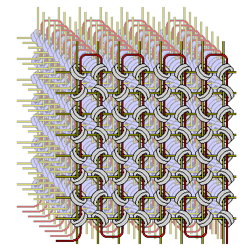
Here, the wire shown in red was used as the sense line for reading, and when data was being written to core, it served as the inhibit line.
The vertical wires, called the X lines, because the one that is used determines the horizontal position or x-coordinate of the core to be selected, have the inhibit line running parallel to them, but in the opposite direction. The X lines for the same column, and the Y lines for the same row, are connected together between all the planes, but the sense/inhibit line for each plane is separate.
A pulse running through the inhibit line for a given plane cancels out the pulse running through the X line for that plane, allowing the contents of a word being written to memory to be controlled.
But wait a moment! We noted above that two pulses will change the data stored in a core, but one pulse is not enough. So it is true that a pulse down the inhibit line will prevent the core in that plane at the intersection of the X and Y lines in use from being written. But what about all the other cores in that plane along the same Y line? Don't they all have two pulses going through them, one through the inhibit line, which is not cancelled, and one through the Y line?
One way to deal with this is to send a pulse that is only half as strong down the inhibit line. If 1 1/2 pulses do not change the data stored in a core, then along the Y line in other planes, the bit that is to be written gets 2 pulses, and the others get only 1 pulse, but in the planes where the bit is not to be changed, all the cores along the Y line with a signal get 1 1/2 pulses.
But it may not be necessary to change the strength of the pulse down the inhibit line, and design the cores to higher tolerances. The pulse going through the inhibit line is opposite in polarity to the pulse going through the X lines, not only in the core where it cancels the pulse through the X line, but in the other cores where there is no signal through the X line to cancel. Because this signal is of the opposite type, its sum with a pulse through the Y line differs in direction by 90 degrees, or a right angle. Thus, while we have a sum that is strong enough to magnetize a core, it is not acting so as to magnetize the core along its circumference; the magnetic field instead crosses the core at right angles, and thus may have no significant effect.
For a short time, fast memories were made using another application of the same principle.
In a thin-film memory, one of the two wires passing by a spot of magnetic material, if the spots in its row were to be selected, always had current flowing in the same direction. The other wire, passing perpendicular to it, could have current flowing either upwards or downwards. The material was fabricated so that it retained magnetism well only in the direcion induced by the wire that could have current going through it in either direction. But the strength of the signals going through the wires was chosen so that it would take both wires working together to shift the magnetism of a spot. Thus, when initially written, the direction of magnetization of each spot was in one of two directions differing by 90 degrees, but it would then settle into one of two directions separated by 180 degrees.
A small signal down the wire through which current flowed only in one direction would disturb the direction of magnetism in the spots temporarily; because the spots were fully saturated, rotating their direction of magnetism was the result, causing a change in the perpendicular direction as well, so that when the magnetization bounced back, a signal went through the other family of wires. This non-destructive readout principle is illustrated below for the form of biaxial core memory sold under the Biax trademark.
The Univac 1107 computer had a small register file, containing a limited number of alternate sets of registers, made from thin-film memory; this comprised 128 words of 36 bits. Several computers made by Univac for military applications had larger thin-film memories.
The IBM System/360 Model 95 computer had a thin-film main memory one megabyte in size, in addition to a supplementary core memory that was four megabytes in size, and was the only IBM computer to use this memory technology. IBM experienced a major struggle in producing a thin-film memory that was not subject to pattern sensitivity, a flaw where some bit patterns cannot be stored properly. The solution found was to cover the memory plane with sheets of a soft magnetic material; these provided a return path for magnetic fields, not dissimilar to that which is intrinsic in the round shape of a magnetic core.
This technology was soon superseded by solid-state memory in any event; the ILLIAC IV, and the ASC (Advanced Scientific Computer) from Texas Instruments were two computers originally planned to have thin-film memories which ended up having semiconductor memories instead.
Incidentally, the later IBM System/360 Model 195 used the same four-megabyte core memory as the Model 95, but this time as its main memory; it had a cache made from semiconductor memory which contained 32 kilobytes, following the success of a cache memory in improving the performance of the IBM System/360 Model 85 computer.
The core memory used on the System/360 Model 95 and 195 had a cycle time of 750 nanoseconds; this was very fast for core memory. In comparison, ordinary core memory might have had a cycle time from 2 to 5 microseconds, and slow core memory, used as "bulk core", might have a cycle time of 10 microseconds. The thin film memory on the Model 95 had a cycle time of 120 nanoseconds and an access time of 67 nanoseconds; in comparison, the semiconductor cache of the Model 195 had a cycle time of 54 nanoseconds.
The speed of core memory, of course, improved during the years in which it was in use. Sometimes, high-speed memories were made using other types of magnetic core than the simple toroidal, or doughnut-shaped, core. For example, rectangular cores with three holes in a line were studied as a possible high-speed core for use on the STRETCH computer from IBM, and cores that were square prisms, with holes running through them at right angles, called biaxial cores, were used as the fast memory for microcode on the Packard-Bell 440 computer, as well as being previously used on the Univac LARC computer for its registers (if I remember correctly).
This diagram illustrates three major forms of nondestructive read-out magnetic core memory that were in use, the transfluxor, the Biax, and plated-wire memory.
On the left of the diagram, we see the transfluxor. This drawing is conceptual; when there is only one small hole, instead of two or four symmetrically distributed around the large hole, the large hole is actually offset to one side to make the path past the small hole wider.
On the top, we see the core magnetized in a clockwise direction as a normal magnetic core. Assuming the core is fully magnetized, or saturated, a current going through the small hole is unable to magnetize a region around the small hole in either direction, because to do so, it would have to more-than-saturate the part of the transfluxor either to the right of it (if clockwise magnetization is attempted) or to the left of it (if counterclockwise magnetization is attempted).
On the bottom, the core has first been magnetized in a clockwise direction by a large current through the central aperture, and then the inner part has been magnetized in a counter-clockwise direction by a smaller current through the central aperture. In this state, it is still impossible for a current through the small hole to magnetize the area around it in a clockwise direction, because then it would have to more-than-saturate the areas to both the left and the right of it, but a current through the small hole can magnetize the area around it in a counter-clockwise direction, since that reduces the magnetization of the parts of the core on both sides.
This makes the transfluxor useful as an amplifying device, since a sense wire also going through the small aperture can determine if a current through a write wire through the small aperture has made any change in the core. Since the change is to a small part of the core, the rest of the core acts as a magnet that restores the change made by currents through the small aperture, so that rewriting is not required when this type of memory is read.
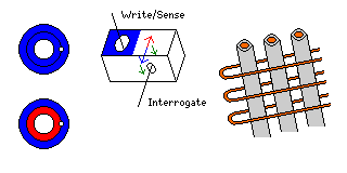
In the middle of the diagram, we see the Biax. The write line goes through the core in one direction, and can create clockwise (blue) or counterclockwise (red) magnetization around it. In a perpendicular line, the interrogate wire goes through the core. If we pass a current through it that leads to a counterclockwise magnetization, the change to the direction of magnetization in the area between the holes is shown by the green arrows.
When the magnetization in the rest of the area around the write line causes the magnetization to spring back to normal, the result looks the same, from the perspective of the interrogate line, whether the magnetization around the write line was clockwise or counterclockwise. A change takes place to the magnetic flux in the direction opposite to the green arrows, or clockwise from the perspective of the interrogate wire.
But from the perspective of the write line, there is an increase in the flux in the direction of the core's original magnetization. (This is because the core was saturated when it was magnetized in the first place, so the current in the interrogate line only changed the direction of the magnetization without increasing its strength.) So the sense line goes through these cores in the same direction as the write line.
The third part of the diagram shows plated-wire memory. The plated wires were the ones through which current flowed in either direction, and they magnetized the plating in the direction in which it would stay magnetized. The wires crossing them had current going through in only one direction, causing a change in magnetization that did not last. This memory worked using the same principle as thin-film memory.
The following diagram:
illustrates both that one could design a thin-film memory that works more like a core memory, and that, in a thin-film memory or in a core memory, if having a factor of two between a magnetic field that does not affect stored information, and one that changes the bit stored, is awkward, one can put additional wires running by each spot, or through each core, with the cost of some additional external circuitry, so that current runs through four wires going through the core being read or written, but at most through only one for any other core. The wires running diagonally belong to the sense line; while using the diagonal line for a five-way coincidence is possible, if a select line and the sense line ran in parallel, the pulse along that select line would produce a strong signal on the sense line.
One of the issues preventing tunnel diodes from being used in fast microprocessors is that they only work if they are in a very narrow range of characteristics, and thus the yield of a chip with more than one tunnel diode on it is unacceptable. A design like the above might make fabrication of integrated circuit memories with zero transistors per cell (although some transistors would be needed, proportional to a constant times log(N) * sqrt(N) for an N-bit chip) practical, by allowing the parameters of the individual magnetic storage elements to vary over a wider range.
The following image:
shows one possible layout for very dense microchips in the future that go beyond the limits of conventional semiconductor fabrication technology.
On the right and the left, as well as the top and the bottom, are shown areas produced with normal semiconductor fabrication techniques that consist of a row and column matrix, with transistors at each intersection. Row and column selection circuitry is not shown.
A series of conductors, more finely spaced than is possible for the fabrication technology that produced the row and column matrix, is shown leaving it at a shallow angle. These form the rows and columns of a different type of row and column matrix that constitutes the main part of the chip. These conductors might be carbon nanotubes, for example.
Since it is assumed not to be possible to use conventional lithography to fabricate transistors at the intersections of this finer row and column matrix, it is expected instead that the coincidence of current in two wires of this matrix will have an effect on the basis of the same principle used in magnetic core memories or thin-film memories.
Instead of placing a continuous sheet of material between the two levels of conductors, possibly there will be a second grid of strings above the top level of conductors, going in the direction of the bottom level of conductors, to allow squares of material to be deposited on the substrate, which might have to be movable by means of microscopic mechanical actuators.
Memories denser than any possible today could be made this way; but an even more exciting possibility is to use this technique to produce field-programmable gate arrays of enormous complexity.
One problem is, though, that a design with only one layer of wiring would be so restricted that the disadvantages of that would outweigh the advantages of a smaller scale. However, the extra layers could all be fixed, and could be built with the help of the mechanical actuators noted above; only one layer of switchable conductors would be enough to allow any type of circuit to be built efficiently. Another problem comes up here; while it would be easy to build a transistor circuit with switchable conductors that would change from being conducting to insulating as well as the presence or absence of a metal layer would do this, or through blowing a fuse, as done with programmable but not erasable read-only memories, partial changes in conductivity due to a magnetic effect require special circuitry to utilize.
Perhaps a simple circuit could use a magnetically-induced change in conductivity to determine if a fuse will be blown.
Another way to improve the performance of future computers, instead of increasing the number of components that could be placed on a chip, would be to produce logic gates that work more quickly in some other way than by making them smaller. For many years, IBM pursued advanced research into the use of Josephson junctions, a type of tunnel diode that relied on superconductivity, as a promising way to make computers operate very quickly, but finally abandoned the effort in 1983. Josephson junctions have been put to commercial use in areas such as sensitive magnetic-field sensors and accurate voltage stanards. In 1995, Konstantin Likharev and several collaborators developed a new way to use the Josephson junction a form of digital logic known as Rapid Single Flux Quantum logic.
The breakthrough that made more effective use of Josephson junctions in digital logic possible was to use circuits that manipulated short electrical pulses rather than producing a continuuous output of voltage to represent a logic state. An experimental microprocessor using this technology operating at a frequency of 20 GHz was built as part of a project supported by the U.S. Government to greatly extend the possible speed of computing some years ago. Because this form of logic is based upon individual pulses, the accuracy of the clock signal is normally critical; if one uses additional circuit elements, however, an asynchronous logic family is possible where both logic 0 and logic 1 involve a pulse, but a pulse sent down a different one of two wires.
As it becomes possible to place more and more transistors on a single chip, the limit to the benefits that can be obtained through making a single processing unit more powerful get reached. Thus, we see chips today that place two or more processing cores on a single die.
What if it were desired to put thousands of tiny computers on a single chip, and to interconnect them as though they were in a large 3-dimensional cube, each computer connected to its six nearest neighbors? The idea might be that such a design could run programs to simulate three-dimensional physical systems, such as the Earth's atmosphere, or even simulate the operation of the human brain, a three-dimensional mass of neurons whose connections are at least somewhat limited by range.
Would even the vastly simpler connections of a 3-dimensional cube, being three-dimensional, overwhelm what is available on the two-dimensional surface of a microchip?
No, as the diagram below illustrates:
Only two layers of metallization are required to allow each cell in the staggered or rotated 4 by 4 arrays in the diagram to connect to the corresponding cell in the next array above or below, and the corresponding cell in the next array to the left or right.
Connecting the cells in the arrays to be connected either along a linear path, making a third dimension, or in a two-dimensional scheme, thereby providing interconnects that have the topology of a four-dimensional hypercube does not require any additional layers, but in practice, instead of squeezing those connections between the connections already present in those two layers, in the area between the cells, the metallization layers used for wiring within the cells will be used instead, allowing both more freedom in positioning the connections and reducing capacitances.
Thus, the problem will be pins to connect between chips, and not connections between processing units on chips.
The way a vacuum tube works is relatively simple and easy to understand. A hot filament is placed inside a metal cylinder. The metal cylinder is called the cathode, and when it is heated, it is possible, if it is kept at a negative voltage relative to a larger metal cylinder surrounding it, the anode, for it to emit electrons. To improve the efficiency of this process, the cathode usually is covered with a special coating; barium oxide is a very good material for this purpose. However, often the cathode itself is made of nickel, and as it happens, under some circumstances the barium oxide will react with nickel to produce an insulating layer around the cathode. This is dealt with by mixing calcium oxide with the barium oxide, and other related compounds such as strontium oxide are usually also present.
This is somewhat reminiscent of the Welsbach mantle on old gas lanterns: a mixture of thorium and cerium oxides also behaves in an unusual way when heated, glowing with a bright white light where other materials, at that temperature, would only glow with a dull red light, as expected from blackbody radiation. (When a Welsbach mantle was originally manufactured, a cotton mesh was soaked in thorium and cerium nitrates; but when the lantern is lighted for the first time, the mantle is converted to the form in which it will be normally used: the nitrates become oxides, and the cotton fibre is burnt away.)
Incidentally, thorium was also often used in vacuum tube manufacture; as the filament needs to get very hot in order to properly heat up the cathode, thoriated tungsten (also used in the rocket engines of the first stage of the Saturn V booster) was often used as the filament material.
Between the anode and cathode, one or more grids may be placed; if the grid is at a negative electrical potential, it will repel electrons going from the cathode to the anode; if it is at a positive electrical potential, it will speed them along their way.
It takes only a small amount of energy to control a large flow of energy, making a vacuum tube an electrical valve, or an amplifier. Incidentally, because both voltage and current are amplified by a vacuum tube, not just their product, power, vacuum tubes can be used in a convenient fashion in electronic circuits without having to convert between direct and alternating current; transistors also have this desirable characteristic (although a bipolar transistor can be used in configurations other than the common-emitter configuration, where one or the other form of amplification is not needed).
Transistors are more complicated to understand than vacuum tubes.
For reasons connected with the nature of the spherically symmetric solutions to Schrödinger's equation in an inverse-square potential, and the Pauli exclusion principle, the electrons orbiting an atomic nucleus organize themselves into "shells". This is the origin of Mendeleev's Periodic Table of the Elements. Except for hydrogen and helium, with an outermost shell with room for two electrons, the outermost shell of electrons for an atom has room for eight electrons. Every atom, in its normal state, has as many electrons as it has protons in its nucleus, since anything that is electrically charged strongly attracts things with an opposite electrical charge. But there is also a weaker effect that means that having an outer electron shell that is completely full or completely empty is also a movement "downhill" to a lower energy state for an atom.
If atoms were isolated from each other, this wouldn't matter, because it is much weaker than the basic electrostatic advantage of being electrically neutral. But if two atoms come close together, one lacking an electron to complete its last shell, and the other just having one electron in its outermost shell, a minimum-energy state can be achieved by the atom with an extra electron giving it to the other atom, and then staying close to the other atom because of the attraction caused by the difference in electrical charge.
This is how atoms combine into molecules; the number of extra, or lacking, electrons in the outermost shell of an atom is called its valence.
In addition to a simple ionic bond as described above, atoms can also share electrons in other, more complicated, ways. In a salt crystal, each sodium atom gives up its extra electron so that each chlorine atom can have an extra electron, but then the sodium and chlorine atoms, attracting each other regardless of where any particular electron came from, form a cubic lattice of alternating sodium and chlorine atoms, so that each sodium atom is joined to six chlorine atoms by, essentially, one-sixth of an ionic bond each.
Silicon, like carbon, has four atoms in its outermost shell. Carbon atoms form strong individual covalent bonds with other carbon atoms, forming structures with definite bonds like graphite or diamond. Silicon dioxide has a structure like diamond's, but with an oxygen atom between each pair of silicon atoms. Pure silicon behaves in a different way; large masses of silcon atoms simply pool all their electrons together.
This is also the way most metals behave, and it is the reason pure silicon is shiny and silvery like a metal in appearance.
Most metals, though, have only two electrons in their outermost shell. In a metal, therefore, the tendency is for atoms to remain aloof from the electron cloud formed by the left-over electrons; it shouldn't get so far away as to leave the metal positively charged, but it can't contribute to making the outer shell complete. (The reason so many metals have two outer electrons is that, from one element to the next, new electrons are being added to a new kind of shell, with room for ten electrons, that is buried within the atom's electronic structure, and does not get involved in chemical reactions.) In silicon, though, the four extra electrons from one atom, plus four others from its neighbor, could also make a complete shell.
If a piece of silicon is peppered with atoms of an element, like arsenic, with five extra electrons, it starts behaving like a metal, because a fifth electron doesn't make sense to the silicon atoms. (Or, to be more precise, since the silicon atoms are arranged in a crystal structure deriving from the fact that they have four extra electrons, the arsenic atom needs to fit in that structure, which leaves its extra electron free.)
If a piece of silicon is peppered with atoms of an element like boron, with three extra electrons, it also becomes conductive, but this time, it is a deficiency of one electron, called a "hole", that is free to move through the substance.
This is because we are dealing with a piece of silicon with a very small amount of the impurity in it, also called a dopant. Thus, the three electrons of the impurity are considered in relation to the electron shell of silicon. A pure substance with three left-over electrons for each atom would tend to let the electrons move about freely, such as the metal aluminum.
A semiconductor diode can be formed by applying opposing impurities to opposite ends of a small piece of silicon. If current flow makes electrons in the n-type silicon flow towards the junction, to meet holes in the p-type silicon also flowing in the opposite direction towards the junction, current can flow. A voltage in the other direction soon causes the vicinity of the junction to run out of charge carriers, both electrons and holes, so the diode's resistance increases.
How can this principle be used to make an amplifier?
The principle of the field-effect transistor is simple enough: if you place a thin metal sheet between insulating layers, and then have a large negative voltage on metal plates outside the insulating layers, the electrical field would force the electrons in the metal conductor in the middle to use a smaller thickness of the metal, thus increasing its resistance. In practice, using metal foils and normal capacitor construction, such a device would produce an extremely weak effect, and not serve as an amplifier.
A field-effect transistor works because it doesn't just rely upon capacitance to put the squeeze on the current flow from source to drain. The junction between the gate terminal and the semiconductor material connecting the source and the drain is a reverse-biased diode. Thus, a field-effect transistor is designed so that if the voltage on the gate terminal is strong enough, the area through which current must flow to go from source to drain is deprived of charge carriers.
But the original form of the transistor, the bipolar transistor, is much harder to understand.
An NPN transistor consists of a strongly-doped area of n-type silicon, the emitter, separated by a very thin gap of p-type silicon, the base, from a weakly-doped area of n-type silicon, the collector.
The junction between the emitter and the base behaves like the junction in a diode; electrons flow only from the emitter to the base.
The base, however, is more lightly doped than the emitter, and it is a very thin region between the n-type emitter and the n-type collector. It is thin enough that electrons flowing from the emitter to the base might continue on into the collector; they will not necessarily collide with a hole in the base, which is the event needed for a flow of electrons in the emitter to collector direction to be converted to a flow of holes in the collector to emitter direction.
Of course, a few of them will still collide. And an electron current in the collector combined with a hole current in the base will lead to the normal situation of a reverse-biased diode. Removing holes from the base side of the collector-base junction also means removing electrons from the collector side of that junction, so that an electron current cannot continue.
But if the holes are supplied by current flow from the base terminal, instead of being taken from the limited supply near the base-collector junction, then this does not develop, and so the current into the base is amplified by the device.
As is well known to users of microscopes and telescopes, diffraction limits the possible resolution of an optical device.
When making integrated circuits, ultraviolet light with a wavelength of about 193 nm is typically used. Since a single wavelength includes one bump and one trough, this is basically enough to allow features that are 97 nm wide to be made on a chip.
Such features, at the very limit of resolution, would be very blurry, however.
The following image

illustrates a smaller amount of blurring than that would cause. The top part of the image shows a mask, and the bottom part the image that would result from using the mask.
The left-hand side of the diagram shows what would happen if one simply made the shape that is desired on the mask; the corners would be rounded off, leading to a different shape being made than that which was drawn.
The right-hand side shows what happens if one pre-compensates for the blurring by making the corners pointy. After blurring rounds the corners, they end up square.
A more sophisticated version of this technique than is illustrated here is called Optical Proximity Correction, and is a standard part of making integrated circuits today.
The edges of the exposures are still soft, of course, but the photoresist used in making chips has a sharp threshold characteristic, like litho film, and so one can produce shapes with straight edges and sharp right-angle corners.
Making ideal shapes, even though their level of detail is still limited by the wavelength of the light used, allows for yet another trick. If one uses multiple exposures, each one producing an idealized shape with features at a width of 97 nm that have nice straight edges and sharp corners, then by offsetting and overlapping the details, one can end up creating details that might, for example, have a width of 33 nm on the resulting chip.
This is the technique known as double-patterning.
As it happens, today's microprocessors, as I write this, have features that are as little as 14 nm in size. So they had to take double patterning further, and use quadruple patterning along with other techniques to make the process self-aligning.
While sand is cheap, high-purity silicon is still expensive.
The wafers of silicon on which microelectronic chips are made are round, while the dies embodying the circuitry of a microchip are square.
As well, the rate of defects is lower near the center of a wafer than it is near the outside.
One way to address both of these realities would be to use a single wafer to make more than one kind of chip, as shown below:
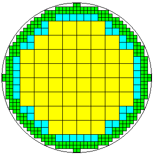
The largest chips are in the center; then, as one goes further out, where there are more defects, smaller chips are made which are less likely to contain a defect, and which can also conform more closely to the round overall shape of the wafer.
At present, however, I think silicon wafers are usually used to make only one kind of chip - with the exception of special runs for student projects, where a wafer might be used to make one each of a large number of chips. They do have to train the future integrated circuit designers of tomorrow somehow.
But in the earlier days of integrated circuit manufacture, this technique was at least occasionally used to make the most efficient use of every wafer.
When all these transistors are put on a tiny silicon chip, that chip is a fragile thing, and so it needs to be put into a little box of sorts to protect it, with pins extending out to carry voltages and signals in and out.
Over time, as integrated circuits grew more complex, this became a more difficult problem.
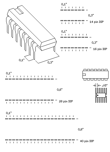
At first, integrated circuits only had a small number of logic gates. The most common sizes of early integrated circuits are pictured here: the 14 pin and 16 pin DIP (dual in-line) packages.
However, the very earliest integrated circuits were in the same metal cans as used for transistors, just with more wires coming out. The dual-in-line package was invented at Fairchild by Don Forbes, Rex Rice, and Bryant Rogers in 1965, as noted on the Computer History Museum web site. They also note a small flatpack package invented by Yung Tao at Texas Instruments; as another page noted, this invention took place in 1962.
A comparison between the size of a DIP and a flatpack package is shown as well in the diagram. Note that while a DIP is designed for insertion, either into a socket, or into holes on a printed-circuit board, the flatpack package was designed to be soldered on to pads on the surface of the board.
Later, wider dual-in-line packages in a similar style were used for more complex integrated circuits. Thus, the 28 pin DIP, where the two rows of pins were separated by 6/10 of an inch, instead of 3/10 of an inch as with the 14 and 16 pin ICs, served for more complex functions, including UARTS. And many of the early 8-bit microprocessors, including the Intel 8080, the Motorola 6800, and the MOS Technology 6502, were usually packaged in the similar 40 pin DIP. (It should be noted that often microprocessors were offered in multiple alternate styles of package for different applications.)
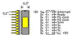
It was possible to put a microprocessor into the kind of small package typically associated with small-scale integrated circuits like the 7400-series TTL chips. And, indeed, the first 8-bit microprocessor, the Intel 8008, was packaged in an 18-pin DIP. This meant that it used a single 8-bit bus for data and addresses, with its contents indicated by the three state bits provided. This bus could contain the most significant 6 bits of an address, the remaining 8 bits of the address, or 8 bits of data.
One value of the three state bits indicated the bus was being used for a transfer of data, but whether that was a read or a write was indicated by the two most significant bits of the byte that had contained the most significant 6 bits of the address which had been sent on a previous cycle.
The chip was made on a PMOS process, and ran at a clock frequency of 500 kHz. It received +5 volts and -9 volts as power, but it could accept normal TTL logic levels as input.
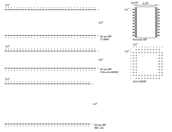
The 8086 and 8088 16-bit microprocessors also used a 40-pin DIP; but some other early 16-bit microprocessors had more pins, for example, 64 pins.
At this point, things began to break down, and alternatives were considered.
The Motorola 68000 simply lengthened the DIP package further; the Texas Instruments 9900 widened it, with the two rows of pins now separated by 9/10 of an inch.
And the J-11 module from DEC, used in both their PDP-11/84 and their Professional 380 computer, which was a powerful PDP-11 essentially equivalent to the PDP-11/70, was even wider, 1.4 inches, even though it had only 60 pins instead of 64. But it was a module - instead of a single die inside a DIP package, it was a ceramic module which had two square packages, each with a die within, mounted on it.
But other approaches started being tried.
Rockwell invented the quad-in-line package, where two staggered rows of pins on each side allowed the number of pins for a package of a given length to be doubled, as the spacing of pins in each row was still 1/10 of an inch.
Intel's 80286 went to a square grid of round pins, separated by 1/10 of an inch in both directions.
This same general style of arrangement, but with more and more pins, served for the 80386, the 486, and the original 5-volt 66 MHz Pentium.
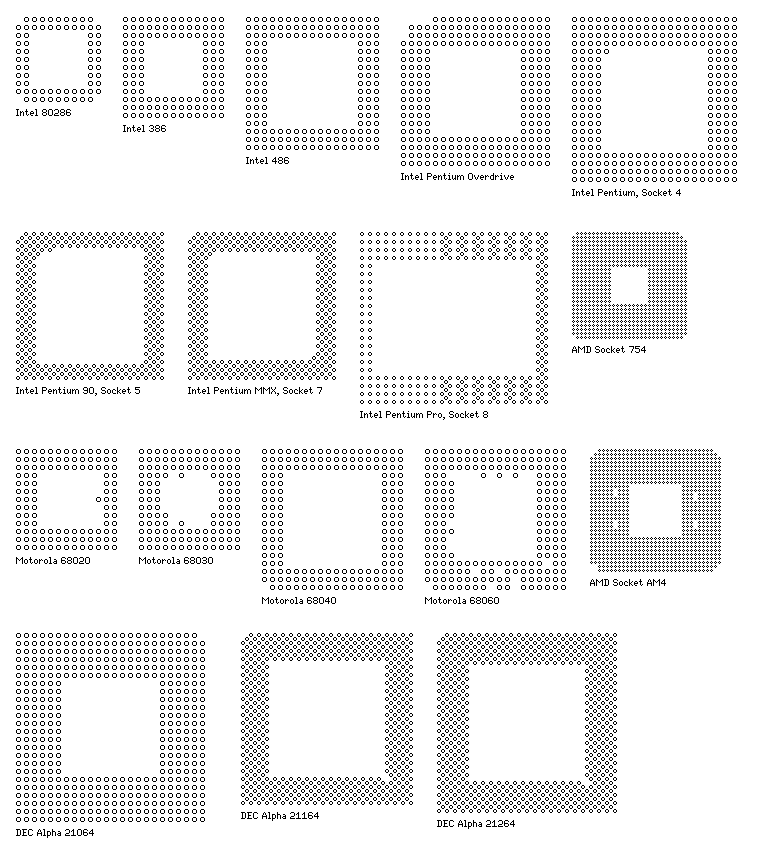
With the introduction of the 90 MHz version of the Pentium, however, Intel moved to a more compact arrangement, with additional pins in the centers of the 0.1" squares formed by pins at the locations previously used. Thus, the minimum distance between pins was divided by the square root of 2.
Socket 5, which was used for this version of the Pentium, had additional holes not corresponding to pins on the 90 MHz Pentium. These were used by early versions of the Pentium with MMX, which later moved to Socket 7, with one additional hole provided.
The Pentium Pro also used what was termed a Staggered Pin Grid Array (SPGA), but in its case, only some of the extra positions were used, and some of the pins still had a full 0.1" spacing.
AMD, beginning with Socket 754, went even further, spacing pins apart by only 1/20 of an inch, 0.05". Intel later did so as well, and has also made chips where the pins are spaced 1 mm apart, at least for mobile devices.
The evolution of the Motorola 68000 line of processors over part of this time period is also shown in the diagram. All of these used a 5 volt power supply except for the last one, the Motorola 68060, which was a 3.3 volt part.
Another historically important alternative to the x86 instruction set is shown, the DEC Alpha microprocessors. When AMD could no longer use the same pinouts for their processors as Intel, after Socket 7, it licensed interfacing technology from the DEC Alpha chips.
Recently, with their experimental neural network chip Loihi, Intel got really creative with the layout of the pins:
Although nicer-looking than my first attempt, I don't know the actual spacings of the pins, this just represents my best guess.