As the Digital Equipment Corporation PDP-8 computer, having originated with a very simple instruction set, was also inexpensive enough that it was the first computer within the reach of many organizations, it holds a place in the affections of many.
Of course, a number of other computers might also have been noted as making computing more affordable, such as the IBM 650, the Bendix G-15, the Packard Bell 250, and the Royal McBee LGP 30, for example. There was more to the enduring affection in which the PDP-8 is held than its affordability, but that is a phenomenon I will not attempt to analyze at length.
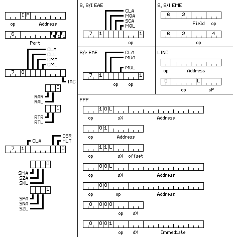
The diagram below shows an overview of the instruction formats available with the PDP-8 and related computers throughout their history:
The first column shows the basic instructions included with the PDP-5 and all PDP-8 models. The opcodes for memory-reference instructions were:
000 AND And
001 TAD Two's Complement Add
010 ISZ Increment and Skip if Zero
011 DCA Deposit and Clear Accumulator
100 JMS Jump to Subroutine
101 JMP Jump
Instead of a store instruction, the DCA instruction cleared the accumulator, so that the TAD instruction could serve the function of the load instruction as well.
The ISZ instruction incremented the number in a memory location, and skipped the next instruction if the result was zero, thus allowing loops to be easily programmed.
The JMS instruction stored the return address in the memory location at the effective address, branching to the following location.
The various input-output instructions, in most cases, used the last three bits to indicate three pulses that could be present during an input/output operation.
The operate instructions, which came in two groups shown in the first column, were:
7200 CLA Clear Accumulator
7100 CLL Clear Link
7040 CMA Complement Accumulator
7020 CML Complement Link
7010 RAR Rotate Accumulator Right
7004 RAL Rotate Accumulator Left
7012 RTR Rotate Two Right
7006 RTL Rotate Two Left

7000 NOP No Operation
7041 CIA Complement and Increment Accumulator
7120 STL Set Link
7240 STA Set Accumulator

7600 CLA Clear Accumulator
7500 SMA Skip on Minus Accumulator
7440 SZA Skip on Zero Accumulator
7420 SNL Skip on Nonzero Link
7510 SPA Skip on Positive Accumulator
7450 SNA Skip on Nonzero Accumulator
7430 SZL Skip on Zero Link
7404 OSR OR Switch Register
7402 HLT Halt

7410 SKP Skip
Note that there are two CLA opcodes, so that the CLA operation can be employed in either group. After the illustrated opcodes for each group, opcodes formed by special combinations of bits are shown in a subsequent list.
The PDP-5 was slightly more limited than the PDP-8 which followed in one way. The rotate instructions could not be combined with most of the other microinstructions, with the one exception that increment could be combined with a rotation by one place, but not two places, and if the halt instruction was present, the skip instructions were ignored. On the PDP-8, the rotates were performed after clear, complement, and increment, and so there was no conflict, and, as well, the halt was performed after the various skip instructions. But the most common combinations of operations were still possible on the PDP-5, such as complement and increment for two's complement, or combinations of two skip instructions.
The Link is the name used on the PDP-8 computer for the carry bit.
When more than one of SMA, SZA, or SNL are indicated, the skip takes place if any condition is met; when more than one of SPA, SNA, or SZL are indicated, the skip takes place only if all conditions are met.
The PDP-8/e added one more opcode:
7002 BSW Byte Swap
which swapped the two 6-bit halves of the accumulator, for convenience in manipulating characters, using an otherwise unused bit combination (don't shift, but do it two places) to indicate this.
The Extended Arithmetic Element was an option for PDP-8 series computers that provided them with a hardware multiply. This option was not conceived of when the PDP-5 was made; thus, the bit, shown as 0, at the end of a Group 2 Operate Microinstruction (an operate instruction of the format including the conditional skip instructions) was ignored for it; the other incompatibility of the PDP-5 was that the program counter, rather than being a special register, was core location zero.
This led to a third incompatibility between the PDP-5 and the PDP-8. On the PDP-5, an interrupt acted like a JMS instruction to location 1 on page zero; on the various models of the PDP-8, an interrupt acted like a JMS to location 0, saving the return address in location zero and taking the next instruction from location one.
On both the PDP-5 and the PDP-8, page zero memory locations eight through fifteen, 10 to 17 octal, were auto-increment locations. When used as indirect addresses, they were incremented before use. This was intended as providing a substitute for an index register.
The original version of the Extended Arithmetic Element, an option available for the PDP-8 and PDP-8/I computers (but not the PDP-8/S and PDP-8/L) had the following opcodes:
7601 CLA Clear Accumulator
7501 MQA Multiplier Quotient Load into Accumulator
7441 SCA Step Counter Load into Accumulator
7421 MQL Load Multiplier Quotient

7405 MUY Multiply
7407 DVI Divide
7411 NMI Normalize
7413 SHL Shift Arithmetic Left
7415 ASR Arithmetic Shift Right
7417 LSR Logical Shift Right

7401 NOP No Operation
The Multiply and Divide instructions took an immediate 12-bit operand following the instruction; as with the JSR instruction, program memory was allowed to be modified. Multiplication took the product of the MQ contents with the operand and placed its most significant half in the accumulator, and its least significant half in the Multiplier-Quotient register. Division starts with a 24-bit dividend in that form, leaving the remainder in the accumulator and the quotient in the MQ.
The three shift instructions, SHL, ASR, LSR, also involved an additional instruction word, giving the number of places to shift, less one.
The normalize instruction places the number of shifts performed in the step counter; it shifts (AC,MQ) until either the first two bits of the AC are unequal, or until the first two bits of the AC are one, and the remainder of the AC and MQ are all zero.
The PDP 8/I did not change the format of the Extended Arithmetic Element instructions, but it did add one opcode:
7403 SCL Step Counter Load from Memory
which took an immediate operand and placed it in the step counter.
With the PDP 8/e, the Extended Arithmetic Element was modified slightly. Even if the optional EAE was not installed, the standard machine had an MQ register, and the MQA and MQL instructions, as well as the version of the CLA that could be combined with them, were included.
Added were the ability to perform 24-bit addition and various 24-bit conditional skip instructions. The function, although not the opcode, of the SCA instruction was changed, but its ability to be combined with other instructions was now more limited, and the SCL instruction was replaced by the ACS instruction.
7403 ACS  Store Accumulator in Step Counter

7441 SCA  OR Step Counter with Accumulator
7443 DAD  Double Precision Add
7445 DST  Double Precision Store
7447 SWBA Switch from B to A
7451 DPSZ Double Precision Skip if Zero
7573 DPIC Double Precision Increment
7575 DCM  Double Precision Two's Complement
7457 SAM  Subtract Accumulator from Multiplier-Quotient
7521 SWP Swap Accumulator and Multiplier-Quotient
These operations are those described as the "Type B" EAE operations for the PDP-8/A, and are presumed to be the correct version of those introduced with the PDP-8/e, although they differ in significant respects from those described in the PDP-8/e Small Computer Handbook of 1971. Two, rather than four, instructions, DPIC and DCM, require two of the other micro-operation bits to be set to function properly. The PDP-8/A EAE also provided for "Type A" EAE operation, which was compatible with the EAE as provided with earlier versions of the PDP-8.
SWBA appears to replace NMU, which would have been "Absolute Normalize", and which was described in the aforementioned 1971 handbook: it is used to switch from mode B to mode A. In mode A, also added in the PDP-8/A and in the final, actual version of the PDP-8/e EAE as well, was the following instruction:
7431 SWAB Switch from A to B
this replaced the combined operation MQL NMI, which would not have produced a sensible result; due to the opcode used, in addition to performing a mode switch, it also performed the MQL operation.
Note that a SWAB operation performed in Mode B also was MQL NMI, and in this case, the NMI simply was not performed, but an MQL was again performed.
Similarly, a SWBA performed in Mode A causes no operation to be performed; it has the form of the combined operation SCA DVI in that mode, which also does not produce a sensible result.
Other changes in the PDP-8/e EAE include that the number of shifts for a SHL, ASR, or LSR instruction was present without an adjustment by one, and the word following a MUY or DIV instruction gave the address of the operand instead of the operand itself.
Input-output instructions were used to operate a module that allowed the PDP-8 computer to have 32K 12-bit words of memory instead of only 4K 12-bit words of memory. The opcodes were:
62n1 CDF n Change to data field n
62n2 CIF n Prepare to change to instruction field n
6214 RDF   Read Data Field
6224 RIF   Read Instruction Field
6234 RIB   Read Interrupt Buffer
6244 RMF   Restore Memory Field
The CIF instruction set the instruction field to change on the next jump instruction. RDF and RIF, if the respective field was n, set the accumulator to xxnx; RIB took the instruction and data fields of the program that was interrupted, and set the accumulator to xxid; RMF restored the fields preparatory to return from an interrupt.
The PDP 8/e version added features useful for running a multi-user operating system. On the PDP 8/I, on the other hand, TSS/8 was supported through the use of a separate option, the KT8/I timesharing option board.
The PDP 8/A added the KT8-A, which could operate in a mode giving compatibility to the earlier memory extension for the PDP-8, or it could extend the memory available to 128K 12-bit words by using five bits instead of three to indicate each of the instruction field and the data field.
The LINC-8 and PDP-12 added a second computer with a different architecture to work side-by-side with the PDP-8 for certain types of data acquisition task. Its instruction formats are briefly shown in the diagram.
One unfortunate characteristic of the LINC architecture, which existed independently of the PDP-8 before the LINC-8 was designed for a data-acquisition machine science laboratories could construct themselves, designed at MIT, was that it performed arithmetic on one's complement numbers, unlike the PDP-8, which used two's complement numbers; this meant that the two architectures could not work together as effectively as might otherwise have been the case.
In the first format, three instructions are provided:
01 ADD Add Contents of Memory to Accumulator
10 STC Store and Clear
11 JMP Jump
The second format makes use of a set of sixteen pointer registers, except that pointer register zero is not used: these are the first sixteen locations of main memory.
The addressing modes for these instructions are:
0 0000 Direct: the address is in the next word of the instruction
1 0000 Immediate: the operand is in the next word of the instruction
0 nnnn Pointer: pointer register nnnn points to the operand
1 nnnn Pre-increment: increment pointer register nnnn, then use it
       to find the operand
A direct address is 11 bits long; the first bit of the following word is ignored in that case.
10000 LDA Load Accumulator
10001 STA Store Accumulator
10010 ADA Add Accumulator
10011 ADM Add to Memory
10100 LAM Link Add to Memory
10101 MUL Multiply
11001 SAE Skip if Accumulator Equals
11010 SRO Skip and Rotate
11011 BCL Bit Clear
11100 BSE Bit Set
11101 BCO Bit Complement
The LAM instruction first adds one to the accumulator if the carry bit is set, and then adds the memory operand to the accumulator, and stores the sum in both the accumulator and the memory location.
The MUL instruction forms a 12-bit product of the memory operand and the accumulator contents; the normally unused first bit of the effective address indicates if the multiplication is done in integer (0) or fraction (1) style.
The SRO instruction rotates the contents of the memory location at the effective address one bit right; if the leading bit was a 1, it skips the next instruction.
The BCL instruction replaces the accumulator with the accumulator AND the inverse of the operand. BSE is an OR instruction, BCO is an XOR instruction.
Another group of instructions has the same general format, but instead of using the addressing modes described, these instructions perform operations involving the indicated pointer register as the destination operand.
00001 SET
00010 XSK
The SET instruction loads a pointer register; if the L bit is clear, from the address indicated; if the L bit is set, from the immediate value given in the instruction.
The XSK instruction skips the next instruction if the last ten bits of the operand are all ones; if the L bit is set, that memory location is incremented before being tested.
Also in this format are the shift instructions. If the L bit is set, the carry bit is included in the shift. The last four bits indicate the number of places to shift the accumulator.
00101 ROL Rotate Left
00110 ROR Rotate Right
00111 SCR Scale Right
The Scale Right instruction performs a right shift; if the carry is included, what is shifted out of the accumulator also goes into the link bit. For both ROR and SCR, what is shifted out of the accumulator is shifted into the Z register, but in ROR it is still only the accumulator, not the accumulator concatenated with the Z register, that is rotated.
There are several other instructions provided with the LINC architecture as well.
Like much else on this page, I only found out about the format of instructions for the PDP-8's Floating Point Processor from Al Kossow's site, which I am somewhat loath to acknowledge simply because it is overloaded enough by its great popularity: and I am told that the floating-point feature of the PDP-8/A computer, a late version of the PDP-8 that had a numeric keypad on the front panel instead of a row of switches, was compatible with it. This processor basically added a second computer to the PDP-8, which worked concurrently to solve floating-point problems. Called the FPP-12, it was made for the PDP-12 specifically, but could connect to the PDP-8/e, the PDP-8/I, and also the original PDP-8 and the LINC-8, and even the PDP-8/L, although not the PDP-8/S or the PDP-5.
The first three lines show the formats of normal FPP instructions:
000 FLDA
001 FADD
010 FSUB
011 FDIV
100 FMUL
101 FADDM Floating Add to Memory
110 FMULM Floating Multiply to Memory
111 FSTA
The bit marked L in the first line of diagram indicates that the index register used is to be incremented after use.
The second line of the diagram shows a short form of memory reference instruction that makes use of a base register. The displacement in the instruction is multiplied by the current operand length in effect so as to make maximum use of the field.
The third line uses the first 24 locations of the area to which the base register points, regardless of the current operand length. The three-bit offset chooses one 36 bit value, the least significant bits of which are used as the address of the instruction. This address may be indexed.
The fourth line, on the original FPP-12, uses only one opcode natively:
01000 JNX Jump if Nonzero Index
which increments an index register (one of eight locations in memory pointed to by an index register pointer) and jumps if the result is nonzero; opcodes 3 through 7 call PDP-8 subroutines which simulate additional instructions.
On the PDP-8/A, only opcodes 3 and 4 call subroutines in this fashion, and there is the additional instruction in this format:
10100 LTR Load Truth
This tests the accumulator, loading either 0 or +1 as floating-point numbers, depending on the same conditions as associated with the jump instructions to be described below.
The fifth line of the diagram shows a number of additional instructions
001000000 JEQ
001000001 JGE
001000010 JLE
001000011 JA
001000100 JNE
001000101 JLT
001000110 JGT
001000111 JAL

001001000 SETX Set Index
001001001 SETB Set Base Register
001001010 JSA
001001011 JSR
The Set Index instruction loads index register 0 from the address field of the instruction; the Set Base Register sets the base register used by instructions whose format is given in the second line of this part of the diagram.
The JSA instruction saves a return address at the beginning of the data block; the JSR instruction stores a two-word jump instruction at its effective address, and then branches to the location following.
The sixth and seventh lines in this section of the diagram show still more instructions:
000001000    LDX
000001001    ADDX

000000001    ALN
000000010    ATX       Accumulator to Index
000000011    XTA       Index to Accumulator
000000100    NOP       No Operation

000000000000 FEXIT
000000000001 FPAUSE
000000000010 FCLA      Floating Clear Accumulator
000000000011 FNEG      Floating Negate
000000000100 FNORM     Floating Normalize
000000000101 START F
000000000110 START D
000000000111 JAC       Jump to Accumulator Contents
The LDX and ADDX instructions have the format shown in the seventh line of the diagram, while the others follow the format in the sixth line of the diagram.
START F and START D switch to operating on three-word floating-point numbers or operating on two-word double-precision fixed-point fractions respectively.
The floating-point unit in the PDP 8/A, although it was very similar, added one very important new instruction:
000--0101 START E
except it called it STARTE, and the START F and START D instructions were so changed as well, which allowed a third mode of operation: double-precision floating-point with numbers containing a 12-bit exponent field followed by a 60-bit mantissa field, for a total of 72 bits.
This was also available as an option for the Floating-Point Processor for the earlier PDP-8 models, and floating-point hardware could be used, within OS/8, by the Fortran IV compiler. The Fortran II compiler also included with OS/8, on the other hand, was based on 8K Fortran, which used a different floating-point format.
This format was called the special floating point format; it was used with 8K Fortran, OS/8 Fortran II, and BASIC on the PDP-8, and, although the FPP-12 could not handle it, a version of the floating-point subroutine package for the PDP-8 was available that did support that format. The usual floating-point subroutine package, however, used the same numerical format as the FPP-12. Both versions of that subroutine package functioned by interpreting floating-point commands having the same format as regular PDP-8 instructions; these interpreted commands had the opcodes:
000 00000 0000  FEXT       Floating Exit         (return to normal instructions)
000 00000 0001  SQUARE
000 00000 0010  SQROOT
000 00000 0011  SINE
000 00000 0100  COSINE
000 00000 0101  ARCTANGENT
000 00000 0110  EXPONENTIAL
000 00000 0111  LOG
000 00000 1011  INPUT
000 00000 1100  OUTPUT
001             FADD       Floating Add
010             FSUB       Floating Subtract
011             FMPY       Floating Multiply
100             FDIV       Floating Divide
101             FGET       Floating Get           (load)
110             FPUT       Floating Put           (store)
111 00000 0000  FNOR       Floating Normalize
The sine, cosine, arctangent, exponential, log, input, and output instructions were only offered in an extended version of the package; although 0007 was called LOG, it calculated the natural logarithm, not the common logarithm. Thus, exactly those transcendental functions were calculated as are normally included in the computer language BASIC.