Having examined, in the previous pages, many old and obscure computer architectures, it would seem only reasonable and fair that I might also deign to examine the architectures of machines in actual use.
However, current microprocessors are somewhat more complex in their addressing modes than many of the older computers, and this does mean that examining them had to be delayed somewhat.
Let us begin with the Motorola 68020 microprocessor. This chip, along with the 360 mainframe, formed part of the inspiration for the ficticious example architecture that is the topic of the next major section in these pages on computing.
While the Macintosh has switched to the Power PC, this architecture is still present in such devices as the Palm Pilot and the TI-92 algebraic calculator.
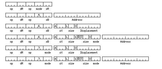
The diagram below very sketchily shows the main addressing modes for a typical memory-reference instruction:
The first line illustrates single-word instructions.
The possible addressing modes are:
000 operand in data register
001 operand in address register
010 address register contents point to memory operand
011 Address Register Indirect Postincrement
100 Address Register Indirect Predecrement
The second line illustrates, with mode 5, the basic memory-reference instruction. One of the address registers serves as the base register, and the 16-bit address serves as a displacement in the region to which it points. In the 68000 architecture, this displacement is a signed two's complement number, so base registers point into the middle of the region they refer to. (The Macintosh simply restricted memory pages to 32 K rather than use negative displacements.)
The third line illustrates the more complex addressing modes offered by the 68000.
The A bit indicates whether a data register (0) or an address register (1) will be used as the index register for the instruction.
The L bit indicates whether the index register will be a 16-bit or 32-bit register.
The size field indicates if the index is to be considered to index in units of 1, 2, 4, or 8 bytes.
This format for indexed memory-reference instructions has an obvious problem. Since the displacement field is only 8 bits long, a base register has to be loaded with a value within 128 bytes of the start of any array; this means that the normal method of allocating a base register to every 64K of memory used by a program is disrupted.
The 68020 corrected this by adding the addressing modes shown in the fourth line.
Here, the not-B bit turns off using the base register, the not-X bit turns off using the index register. The second size field indicates the form of the address:
01: no address
10: 16-bit address
11: 32-bit address
and the mode field controls if indirection, with pre-indexing or post-indexing, is used. Indirection with post-indexing allows an indirect reference to an array; indirection with pre-indexing allows choosing from a list of addresses.
The fifth and sixth lines deal with additional modes, for example, program-counter relative addressing and absolute addressing (thus, address register 0 can be used as a base register).
In the ColdFire architecture, derived from the Motorola 68000, the indirect postdecrement and preincrement modes are omitted. Also, the size field can only specify indexing in units of 1, 2, or 4 bytes. Most arithmetic and logical instructions can only operate on 32-bit operands. The multiplication and division instructions are changed and limited, and several other instructions are omitted. And the forms of the indexed instructions with 16-bit displacements introduced with the 68020 are again omitted from the architecture.
Of course, Macintosh computers later came to use the PowerPC chip instead of the 68000 and its descendants, a chip which is also popular in workstations.
The following illustration shows some of its instruction formats, along with those of two other RISC architectures of recent vintage:
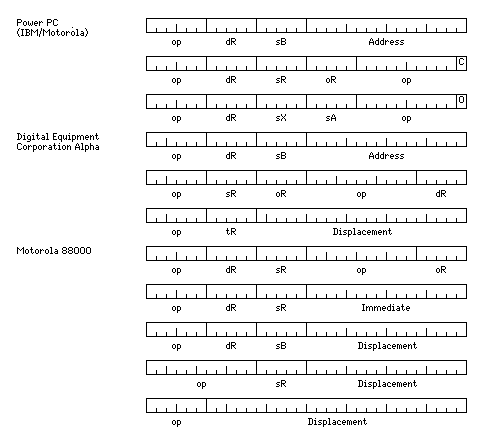
It has 32 general registers, which allows operations to take place largely between items in registers. It also has a classic load-store RISC architecture, so that all arithmetic instructions involve operations between the registers only.
The first line indicates the format of a standard memory-reference instruction, the second that of a register-to-register instruction. The C bit indicates whether or not the instruction is to be permitted to update condition codes.
There is a load address instruction having the format of a memory-reference instruction; this is useful in preparing to use the instruction whose format is given in the third line: a memory-reference instruction where the contents of two registers are added to obtain the effective address. This substitutes for the fact that the regular memory-reference instruction does not include a position for an index register in addition to a base register.
The second set of instruction formats shown in the illustration above are from the Alpha family of microprocessors originally developed by the Digital Equipment Corporation. This architecture uses a set of 32 general registers which can also serve as base registers. Three instruction formats are shown. The memory-reference format, used only for loads and stores, specifies one register as the destination of loads and the source of stores, another as a base register, and has a 16-bit address. Arithmetic instructions are three-address instructions, with all their operands in registers, and have an 11-bit field for specifying the operation to be performed. Branch instructions specify a single register of which to test the contents, and have a 21-bit program-relative displacement. The Unconditional Branch instruction places a return address in the register specified by that field, and Jump instructions, having the same format as the load and store instructions, are used for returning from subroutines.
The third set of instruction formats shown is that of the Motorola 88000 series of microprocessors. This architecture, like the two others in the illustration, uses 32 general registers. A large number of general registers is a characteristic of RISC architectures; some have 128 or even 256 registers, but 32, generally seen as the minimum, is popular.
The 88100 used the same register file for floating-point and integer operations, which was considered to be an unfortunate decision because this, by requiring more circuitry to be connected to the main registers, placed limits on the speed with which information could go from them to the various ALU circuits. The 88110 introduced an additional separate floating-point register file.
A recent exciting addition to the Power PC family has been the CELL processor. This processor chip contains one full PowerPC core, accompanied by eight additional cores on the same chip. These additional cores, termed Synergistic Processor Units, do not access memory external to the chip. They also do not perform input-output, nor do they have any privileged operations. As well, while they perform both single-precision and double-precision floating-point operations using the standard IEEE-754 floating-point format, they do not support all the features of that standard.
Each of these cores has 128 registers that are 128 bits in width. Those instructions that act on a single quantity at a time, instead of multiple values at once in typical AltiVec fashion, do so on a quantity that is right-aligned within the leftmost 32 bits of the register.
The instruction formats of these cores are not the same as those of the PowerPC architecture, but are instead:
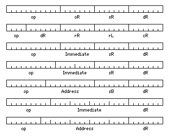
although in this diagram, purposes have been given to the various fields that represent only one possibility for each given format. Thus, in the second line, the register cR contains bits that select portions of the 256-bit concatenation of rL and rR to place in the register dR.
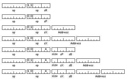
Next, here are the formats for memory-reference instructions for the Intel 80386 microprocessor and its successors:
which, of course, is likely to be the hardware architecture of the machine most readers of this page will actually be using, even more so now that current Macintosh computers also use chips of that type.
Not shown in the diagram is the fact that some instructions will include an additional prefix byte as part of the opcode.
The formats in the bottom three lines are only applicable in 32-bit addressing mode, and thus are not applicable to the original 8086 architecture.
The size field indicates the scaling applied to the index register; again, it is in units of 1, 2, 4, or 8 bytes.
Immediate addressing is present for many instructions, but this is indicated by the use of a different opcode. The first four 16-bit registers have the eight 8-bit registers as their halves, and several of the eight 16-bit registers have special functions.
The original 8086 had an address space of one megabyte, requiring a 20-bit address, but all addresses were only 16 bits long. This was achieved by the use of segment registers, also 16 bits long, which pointed to the beginning of a 64K area starting on a 16-byte boundary, used for a particular purpose, such as for code, for data, or for the stack. There was also an extra segment, that could be used for an instruction's operand by the use of a prefix byte.
And the following diagram illustrates, in a very brief and superficial manner, the instruction formats of the Intel Itanium microprocessor:
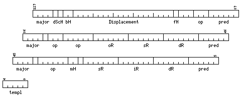
A 128-bit instruction bundle consists of a 5-bit template field which indicates both parallelism and which functional units of the chip are used by the three components of the instruction, and three 41-bit instruction words.
Because little-endian operation is the default, the first instruction executed is the rightmost one. The slope of the diagram is an attempt to illustrate this; bits are numbered from 0 to 127 from right to left, and thus the lefttmost bits are at the top of the diagram, but the slope moves the instruction shown at the top to the right, indicating it is the third instruction to be executed.
All instruction words begin with a four-bit major opcode, which indicates the general purpose of the instructions, and nearly all end in a six-bit predicate field, which allows one of sixty-four flags to control if the instruction is executed.
The first 41-bit instruction element executed, shown in the third line in the diagram, is given a typical M-unit format, the M-unit performing data movement instructions; the second, a format typical for I-unit or F-unit instructions that perform arithmetic; the third one executed, shown in the top line of the diagram, a format typical of the B-unit formats that specify branches. For such an instruction bundle, the five-bit template field could contain either 10000 or 10001 if the middle instruction was an integer instruction, or either 11100 or 11101 if the middle instruction was a floating-point instruction.
The example M-unit format shown above includes the mH field with a move hint, a source register sR, a destination register dR, and an increment register iR.
The example arithmetic instruction shown as the second 41-bit instruction element specifies source, operand, and destination operands in sR, oR, and dR. Several bits are used to specify the opcode.
The third 41-bit instruction element is given one of the B-unit formats. It includes a branch hint bH indicating if the branch is likely to be taken, plus a cache hint cH and a prefetch hint fH. The 20-bit displacement is expanded to 21 bits by a displacement sign dS which is not contiguous with it.