On the previous pages, the history of computers has been recounted by looking at different computers that were used in different periods of time.
In the era of the microcomputer, though, the question might well arise, what is really the computer? The box that sits on a table, or the chip inside that box that actually does the computing?
And, as noted on a preceding page, when most computers are just slightly different implementations of one standard architecture, it really is the chip inside that represents what has changed from one time to the next.
It's already been noted when the chips were originated that started the microcomputer revolution: the 8008 dates from 1972, and it was the first chip that could make a microcomputer possible, and indeed, some microcomputers based on that chip were made and sold.
The Intel 8080 appeared in April, 1974. It was superior in a number of ways: it had a 40-pin package, not an 18-pin package, so the address and data buses did not need to be multiplexed on top of one another, and it could address 65,536 bytes of memory instead of just 16,384 bytes of memory.
The Motorola 6800 appeared later in 1974, and the MOS Technology 6502 was launched the next year, 1975, as a less-expensive alternative to the 6800.
The Intersil 6100, an early processor built on the CMOS process, which was an implementation of the PDP-8/e instruction set, came out in 1975 as well.
It was in June 1976 that the Texas Instruments 9900 came out. This was the first 16-bit processor. It came in a 64-pin package. To make it possible to put a 16-bit processor on a single die with the technology of that time, while the instruction set used sixteen registers, each 16 bits long, those registers were in main memory. Only the program counter, the status word, and a workspace pointer, which pointed to the area in memory used for the registers, were on the chip.
This design had the advantage of allowing very rapid context switching.
In July, 1976, Zilog introduced the Z80. This chip was compatible with Intel's popular 8080, but it also introduced a number of extensions to the instruction set. However, the major additional feature that led to it becoming very successful was that it included circuitry on the chip to perform DRAM refresh, significantly reducing the cost and complexity of systems based on it that used dynamic RAM.
I only recently learned, and was shocked to find out, that the Zilog Z80 only had a 4-bit ALU internally.
In 1977, National Semiconductor brought out the MM57109, in an attempt to address the desire of hobbyists building systems with 8-bit microprocessors to add the mainframe-like capability of hardware floating-point to their systems. However, this chip performed floating-point operations more slowly than doing them in software - so its only benefit was to save on programming. This was because this chip, although it was designed to interface to a microprocessor, instead of sensing the keys of a keypad, and driving a seven-segment display, was still the same as a scientific pocket calculator chip when it came to the part that actually did arithmetic! Understandably, it was largely recieved with derision.
Also in 1977, AMD came out with the Am9511. This was also a floating-point accelerator chip designed to be used with 8-bit microprocessors, but this one provided a genuine hardware floating-point capability. Understandably, it was expensive. Unfortunately, as well, it only performed operations on single-precision 32-bit floating-point numbers. Thus, while it was an admired and respected product, its sales were limited. In 1979, the Am9512 supported double-precision arithmetic, but dropped log and trig functions, to remain within what could be manufactured at the time.
In 1978, Motorola introduced the 6809, an 8-bit microprocessor similar to their previous 6800, but with the advanced feature of multiplication in hardware. As it arrived relatively late in the 8-bit era, it was only used in a limited number of computers aimed at the consumer, such as the Radio Shack Color Computer.
The Intel 8086, a 16-bit chip which did not need to resort to placing the registers off the chip, was released on July 1, 1979. The 8088, a version of the 8086 which had an external 8-bit data bus instead of an external 16-bit data bus, was released on the same day, which led to the latter chip being adopted for the IBM PC.
The Motorola 68000, a 16-bit chip with an elegant architecture, became available afterwards in 1979. The Motorola 68008, a version with an external 8-bit data bus, eventually became available in 1982; so it did not get to be used in the IBM PC, only in the far less successful Sinclair QL.
In 1980, Intel announced the 8087, a floating-point coprocessor for the 8086 and 8088 chips. Intel developed the IEEE 754 floating point standard as part of its work developing the chip. The 8087 had an eight-element stack within it, rather than containing addressable floating-point registers; this allowed it to perform most common floating-point operations with less communications bandwidth being required between the 8087 and the main CPU to which it was attached.
The Intel 80286, a successor to the 8086, was introduced on February 1, 1982. This chip was notable for offering protected mode, which was suitable to advanced operating systems. However, when the chip was in protected mode, it was unable to execute programs written for the original 8086, and changing to the compatible mode requred a complete restart of the chip. That meant that while the 80286 could run new advanced operating systems, it could not run a new advanced operating system that could also run all one's existing programs for MS-DOS or PC-DOS.
Therefore, while a UNIX-like operating system was made that could run on the 80286 in protected mode, the availability of the 80286 could not, and therefore did not, lead to DOS being upgraded to offer more advanced features; it had to steadfastly remain in real mode and eschew the use of protected mode.
The Motorola 68020 came out in 1984. This added a base plus index addressing mode with 16-bit displacements to the 68000 instruction set (which only allowed using both a base and an index if the displacement shrank to 8 bits), and in other ways exemplified a full 32-bit architecture. Unlike the 68000, it was made on a CMOS process, reducing its power consumption.
At this point, microcomputers could be thought of as cheaper alternatives to mainframes instead of cheaper alternatives to minicomputers.
Also in 1984, Motorola brought out the 68881, its floating-point processor for the 68000 and the 68020. Later, perhaps in 1987, it brought out a (mostly) compatible but improved version, the 68882. The instruction set and pinout were the same, but when saving its internal state, it used more space, which meant that some software would have to be updated to use it.
In 1985, Intel brought out the Intel 80386. This was a tremendous advance over the 80286. While the 80286 could address up to 16 megabytes of memory with a 24-bit address, the 80386 had a full 32-bit address bus.
Also, it offered "Virtual 8086 mode", which allowed a version of Microsoft Windows for the 386, as it later came to be known, to be made which offered the ability to use a large memory, other protected mode features, along with the ability to run DOS programs without problems.
The year 1992, which, as we saw on the previous page, was notable for the introduction of Windows 3.1, which proved to be very successful, transitioning the IBM PC platform from being one with a command-line interface to one that, like its competitor the Macintosh, had a Graphical User Interface (GUI). However, Windows 3.1 was still a program that ran under DOS; normally, after booting up into DOS, one started Windows by typing "win" at the command prompt, like this:
C:>win
It was only on August 24, 1995 that the transition of the IBM PC platform away from the DOS command line to a GUI was completed with the availability of Windows 95. Of course, though, while it wouldn't be needed much in normal day-to-day computing, unlike a Macintosh, a computer running Windows still had the ability to open what was basically a terminal window in which the Command Prompt was available; this was true for Windows 95, and it is still true for Windows 11, although now there is also Windows PowerShell.
That year is also notable for the introduction, by the Digital Equipment Corporation, of the Alpha AXP 21064 microprocessor. This microprocessor, like several other RISC processors, avoided the use of condition code bits. It was one of the earliest chips to have a 64-bit architecture. Because it was a very high-performance design, representing the peak of what was possible to put on a single chip at the time, it was also quite expensive, and that limited its popularity in the marketplace, but it is remembered for the many innovations which it embodied.
That is not to say that nothing happened between 1984 and 1992. July 1985 marked the availability of the Atari ST computer, and in early 1986 one could get one's hands on an Amiga 1000. So there were GUI alternatives cheaper than a Macintosh before 1992, but this was one that just involved buying software for the computer you already had, the computer that was the standard everyone else was using for serious business purposes.
In 1989, the Intel 80486 chip came out; unlike previous chips, it included full floating-point hardware as a standard feature right on the chip, although later the pin-compatible 80486SX was offered at a lower price without floating-point.
In February, 1990, IBM released its RS/6000 line of computers. They were based on the POWER architecture, which later gave rise to the PowerPC. This RISC architecture had multiple sets of condition codes to allow the instructions that set conditions to be separated from conditional branch instructions, reducing the need for branch prediction.
The high-end machines in the RS/6000 line used a ten-chip processor, the RIOS-1, notable for being the first microprocessor to use register renaming and out-of-order execution. This technique was invented by IBM for the IBM System/360 Model 91 computer. That computer had several immediate descendants, the 95, the 360/195 and 370/195, but after them, IBM did not make use of this groundbreaking technique in its computers for a while. This has been perceived by some as an inexcusable oversight on their part, but given that this technique is only applicable to computer systems of a size and complexity that, until recently, were associated only with the very largest computers, it should be more appropriately viewed as a natural consequence of IBM making the computers that were relevant to its customers within its core business.
And IBM did make use of out-of-order execution when appropriate, and often before others.
And then out-of-order execution was again used, first in the RIOS-1, as noted, in 1990, and then in IBM mainframes in the IBM ES/9000 Model 520, from 1992. It was again used with the G3 CMOS processor in the 9672 processor in the ES/9000 family in 1996.
The RIOS-1, like the 360/91, only used OoO for its floating-point unit; the same was true of the Pentium Pro and Pentium II processors, which introduced this technique to the world of personal computers.
Out-of-order execution was first used in CMOS single-chip processors implementing the zArchitecture with the z196 from 2010.
In 1993, Intel offered the first Pentium chips, available in two versions, the full 66 MHz version, and a less expensive 60 MHz version. These chips were criticized for dissipating a considerable amount of heat, and there was the unfortunate issue of the floating-point division bug. These chips were pipelined, but in-order, in both their integer and floating-point units.
In 1994, the last chip in the Motorola 680x0 series was introduced, the 68060. Its integer unit, but not its floating-point unit was pipelined (with an in-order pipeline). This processor was never used in any Apple Macintosh computers (or, more correctly, no Apple Macintosh computers were manufactured with that chip; there were third-party upgrade boards that let you replace the existing 68040 processor in one with a 68060 and some interface circuitry), as Apple began selling Macintosh computers using the PowerPC chip instead in March 1994.
As a result, the 68060 never made much of a splash in the market, although there were a few high-end Amiga computers, such as the Amiga 4000T, that used it. There was even a motherboard, the Q60, made by a German company, that could fit in a PC case and which allowed one to run the operating system from the Sinclair QL computer with the 68060 chip.
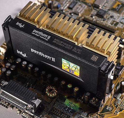
The Intel Pentium Pro chip was announced on November 1, 1995. This design was optimized for 32-bit software, and was criticized for its performance with the 16-bit software that most people were still using. The later Pentium II, introduced on May 7, 1997, resolved that issue, but was otherwise largely the same design, but of course with improvements. However, unlike the case with the Pentium Pro, the cache ran at a slower speed than the processor.
A Pentium II appears in the photograph shown at right, installed in a motherboard, in a detail from a photograph graciously released into the public domain on the Wikimedia Commons by the user Oligopolism. The Pentium II in the photograph isn't the original model in that series, but a later one that ran at 400 MHz instead of 233 MHz. The fins of the heat sink are in their plain copper color, instead of black, and have a different geometry than in the first Pentium II.
The Pentium II had cooling requirements that were much greater than those of previous chips, with presumably the exception of the Pentium Pro, which was why Intel chose to switch from a conventional socketed design to the Slot I design: this was the simplest way to ensure that these requirements would be met in a world unfamiliar with the increased cooling requirements of the newer processors. The Pentium III also used the Slot I design, but then it was no longer needed, as computer system manufacturers and third-party CPU fan makers were prepared to address the cooling requirements of the newer CPUs. Or perhaps even to take those cooling requirements seriously, rather than assuming they couldn't possibly be anything but a misprint, as could easily have happened at the beginning of such a dramatic increase in the cooling requirements of CPUs.
Further improvements appeared in the Pentium III. A hardware random-number generator was included in the support chipset for that processor, as part of a feature which included a serial number on the chip that software could read. Although that feature could be disabled, it was controversial; the intent was to facilitate the distribution of software that had to be well-protected against piracy or misuse (i.e., software to display protected content under controlled circumstances).
The Pentium Pro was available in different versions; a 150 MHz version used a processor built on a 500 nm process (or 0.5 micron), while a 200 MHz version used a processor built on a 350 nm process.
The AMD K5 microprocessor was also out-of-order, and was introduced in 1996, not long after. It initially had bugs in branch prediction and caching, but these were later resolved. Even after the bugs were corrected, it was never very successful, unlike the K6, its successor. The K5 was largely based on the Am29050, a version of the AMD Am29000 RISC microprocessor. As this high-performance processor was used in avionics, when AMD decided to cease development of the 29000 series, it sold the design to Honeywell, which still makes products in the 29KII family to this day. 29000 microprocessors were also used in some laser printers.
The 29050 was the only out-of-order member of the 29000 family; this chip was introduced in 1990, and so it predated the Pentium Pro. However, the Intel 80960CA, from its i960 lineup, was introduced in 1989, and was also superscalar, but unlike the 29050, it required a coprocessor for hardware floating-point.
The AMD K6, introduced in 1997, was based on the NextGen Nx686, and thus resulted from AMD's purchase of that company. Unlike the K5, it was a success, and thus allowed AMD to provide serious competition to Intel.
Early articles about the K6 said that it was intended to be the first x86 chip with multimedia instructions. But Intel released its own chips with MMX instructions before the K6 came to market, so the K6 supported MMX rather than a multimedia instruction set of its own. MMX divided up a 64-bit vector into multiple integers that were shorter in length; it didn't provide for two 32-bit floating-point numbers in that space. In 1998, AMD came out with the K6-2, with special instructions of its own, the feature being called "3D Now!", to add this feature. When Intel's own SSE provided floating-point capabilities as part of the de facto standard, AMD switched over, although also providing 3D Now! support for a while to allow use of older software specifically designed for AMD chips.
The Pentium 4 chip, introduced on November 20, 2000, was a completely new design. It had fewer gate delays per pipeline stage. This meant that the chip's cycle frequency was faster, but instructions took more cycles to execute. At the time, this sounded to people like it was a marketing gimmick instead of an improvement. In fact, though, it was a real improvement, because the Pentium 4 was a pipelined chip with out-of-order execution, intended to issue new instructions in every single cycle, rather than waiting to perform one instruction after another: therefore, a higher cycle frequency did mean that more instructions were being performed in a given time, as long as the pipeline could be kept just as full.
But initially it required the use of a new and more expensive form of memory, which did not help its success in the market.
Intel's subsequent chips in the Core microarchitecture went back to many aspects of the Pentium III design for an important technical reason: shorter pipeline stages meant that the transistors on the chip were doing something a greater fraction of the time. This would produce more heat, and the characteristics of newer, smaller integrated circuit processes were not proving as favorable as hoped (this is known as the demise of Dennard scaling), and so a similar design on a newer process would have dissipated more heat than it would be practical to remove.
Some sources give a date of 2006-2007 for when Dennard scaling came to an end; looking at a graph of how clock speeds improved in processors, it seemed to me as if the transition from rapid progress to a much slower pace that shortly came almost to a stop took place in 2003. A closer look at what was going on at the time, though, shows that the high clock rates seen in 2003 were due to the design characteristics of the Pentium 4 processor of that period.
And, thus, other means of increasing performance were needed, and we entered the era of dual-core and quad-core microprocessors.
IBM came out with a dual-core PowerPC processor in the POWER4 series in 2001.
It was not until May 2005, though, that Intel released the Pentium D and the Pentium 840 Extreme Edition, and AMD released the Athlon 64 x2 on May 31, 2005; but a dual-core Opteron was released on April 21.
The first Core 2 Quad processor was the Extreme Edition QX6700, introduced in November 2006; it was followed by one "for the rest of us" in January 2007, the Q6600.
The Q6600 was a 65nm chip, with a clock frequency of 2.4 GHz, making it not too different from contemporary chips in raw speed, even though today's chips are on considerably smaller process nodes.
These early quad core chips were a multi-chip module with two dual-core dies in one package; in March 2008, AMD released a monolithic quad-core Phenom processor. However, the Core 2 Quad already had Hyper-Threading, whereas AMD did not introduce SMT to its line-up of processors until much later with Ryzen. And the original Threadripper 1950X from AMD used two eight-core dies to achieve its sixteen cores, while Intel's 18-core i9-7980XE was monolithic.
For comparison, in May, 2003, Pentium 4 chips with clock frequencies of up to 2.8 GHz on a 130 nm process were released.
In both cases, shortly after, more expensive versions with even higher speeds were released, these are merely the top-speed chips considered to be part of the "mainstream". Since the Pentium 4 achieved a high clock rate by using unusually short pipeline stages, however, the fact that similar clock speeds were subsequently achieved by the Core 2 design (which was viewed at the time as a return to an internal design, or microarchitecture, similar to that of the Pentium III) would imply that the move from 130 nm to 65 nm did make the logic gates faster, making it correct to view 65 nm as the point at which Dennard scaling came to an end.
We don't have to guess, however. Pentium III chips were also produced on a 130 nm process, and they went up to 1.4 GHz in speed, half the clock frequency of Pentium 4 chips made on the same process.
The Core 2 Duo E6850, manufactured on a 65nm process, offered a clock speed of 3 GHz, but the Core 2 Quad Q6700 offered 2.67 GHz.
At 45nm, one could go up to 3.33 GHz, although the Core 2 Quad Q9650 went up to 3 GHz, so, again, quad-core processors were limited to lower speeds than dual-core processors on the same process. At 32nm, up to 3.4 GHz, at 22nm up to 3.5 GHz, so process in clock speed was very gradual after that point.
Initially, finding a suitable light source for integrated circuit lithography was not a serious issue. The wavelengths of visible light were much smaller than the feature sizes that were attempted.
A mercury vapor lamp was a very common and convenient light source for this purpose. Initially, the g-line of mercury, at 4358.328 Å or 435.8328 nm was used. This was entirely suitable for the manufacture of microcircuitry down to the 1.4 um process node.
Eventually, as feature sizes decreased, other spectral lines with shorter wavelengths were used instead: the h-line, at 4046.563 Å or 404.6563 nm, and the i-line, at 3650.153 Å or 365.0153 nm. The i-line, although in the ultraviolet, was still convenient for making chips with 800 nm features.
In 1982, Kanti Jain, at IBM, demonstrated the excimer laser. Krypton Fluoride excimer lasers provided light with a wavelength of 248 nm, which allowed considerable further progress in making microcircuits with still smaller features. Eventually, there was a shift to Argon Fluoride excimer lasers; they produced light with a wavelength of 193 nm. This was in the far ultraviolet range (as opposed to the KrF excimer laser, the light of which was in the UV-C range), and permitted further progress.
Shorter wavelengths of light may be produced with excimer lasers: a Fluorine excimer laser can produce light with a wavelength of 157 nm, and an Argon excimer laser can produce light with a wavelength of 126 nm. However, while there was some effort made to produce Fluorine excimer lasers, because air was now opaque to this shorter wavelength of light, the relatively small gains from using this type of ultraviolet light were ultimately thought to be not worth the effort, particularly with EUV on the horizon.
Instead, the semiconductor industry shifted to immersion lithography with the existing 193 nm wavelength of light. Immersion lithography reduces the effective wavelength of the light used by dividing it by the index of refraction of the liquid in which immersion takes place.
And when EUV failed to arrive as soon as expected, feature sizes continued to shrink. The most effective of the measures used to achieve this was double patterning, and its successor quadruple patterning.
Earlier on, before there was as serious a conflict between the desired feature sizes and the available wavelengths of light being used, a special technique called Optical Proximity Correction had been developed. Normally, to produce an image with details that are, say, 300 nm wide, one doesn't just need to use light with a wavelength of 600 nm; instead, light with a wavelength of 200 nm is preferable, so that in addition to the fundamental, the third harmonic is covered. 120 nm, to also have the fifth harmonic, would be even better. Otherwise, if one uses a wavelength of light just barely adequate to the amount of detail it is desired to create, the result will be blurry, with rounded corners and so on.
Optical Proximity Correction puts spikes into the corners of the original optical mask in order to compensate for the effects of a wavelength limitation.
Thus, it was possible to make a chip with traces that were at the limit of what was possible given the wavelength of light used to print those details on the chip, and yet have those traces also have straight edges and sharp corners, even though that involves control over detail which is smaller in size than the traces themselves, which would seem to be impossible if those traces are at the limit imposed by diffraction.
Double Patterning used this ability by exposing a chip to light with two different masks, and timing the exposures so that only those areas illuminated in both exposures were affected by the light used.
This made it possible to print details on a chip that were one-third the size of those that could be printed in a single exposure, at the cost that there were restrictions on what shapes could be drawn - making chip design in processes using double patterning much more difficult.
Also, other measures which did not reduce the feature size were used to increase the density of circuits on a chip; so chips advertised as "10 nm" or "7 nm" actually had feature sizes of 18 nm or 20 nm, but compared to older chips where the designation matched the feature size, the increased circuit density was proportional to the designation.
It was only in 2017 that ASML achieved the goal of making an EUV lithography system, using a 13.5 nm wavelength of light, more than ten times smaller than what had been in use, available to the semiconductor industry.
Some of the types of excimer laser mentioned above might sound silly, at least to people who learned their chemistry from out-of-date textbooks. Argon and Krypton are two of the inert gases, Helium, Argon, Neon, Krypton, Xenon and Radon. So why are chemical compounds involving them being mentioned?
Ammonia has the chemical formula NH3; a molecule of ammonia has one atom of nitrogen, and three atoms of hydrogen. This is because the outer shell of the nitrogen atom has five out of a possible eight electrons in it, and so by taking one electron from each of three hydrogen atoms, it can achieve a complete outer shell.
Hydrogen and helium are special; their outermost electron shells have room for a possible two electrons instead of eight. So the hydrogen atom, with one out of two electrons, if given an extra electron, also has a complete outer shell, and is happy, but taking away an electron works just as well.
However, because the force of the desire of atoms to have a complete outer shell is weaker than the electrostatic force, which inclines atoms and other things to stay electrically neutral, this kind of electron sharing only works when the atoms involved stick closely together, forming a molecule.
This is an oversimplified picture, but it explains the pattern of the Periodic Table of Elements. The source of the table, ultimately, is the behavior of electrons around the nucleus in an atom, as it results from quantum mechanics.
Helium is an inert gas, because it is happy with two out of two electrons in its outermost electron shell, and Argon, Neon, Krypton, and Xenon are inert gases, because they're happy with eight out of eight electrons in their outermost electron shells.
The halogens, Fluorine, Chlorine, Bromine, Iodine and Astatine, have seven electrons in their outer shells, so they're very hungry for the one electron they need to be happy. The earlier elements in the list, which are the lighter ones occuring earlier in the Periodic Table, are the most hungry.
Thus it is that while xenon is an inert gas, happy with eight electrons in its outer shell, it's still possible, by exposing xenon to fluorine, to produce xenon fluoride. However, xenon fluoride doesn't have the formula XeF8, as one might expect, so the story gets more complicated.
In any case, when the chemist Neil Bartlett first synthesized a form of xenon fluoride in the early 1960s, this caused a sensation, because up to that time, it was believed that the inert gases were absolutely inert chemically.
There was a famous essay by Isaac Asimov, in which he explained why this wasn't discovered sooner: because of how deadly, and therefore difficult to work with, the element fluorine is. And because xenon was rare and expensive until recently as well.
As well, some dates to provide a frame of reference for the progress in bus connectors in processors might be in order.
In the original IBM PC, in 1981, memory was either added in sockets on the motherboard, or by means of memory cards that plugged into the standard peripheral bus, which was also used for video cards. The IBM Personal Computer/AT from 1984 included a revised bus with an extended connector that was upwards compatible, adding support for a larger address bus, and for a 16-bit data bus instead of an 8-bit data bus.
After the IBM Personal System/2 introduced the Micro Channel bus in 1987, a competing standard, EISA, was offered by other computer manufacturers to offer similar features but with upwards compatibility with older peripherals.
Then the PCI bus was introduced by Intel in 1992, originally in a 32-bit version.
By 1986, 30-contact single in-line memory modules (SIMMs) were used with AT-compatible computers and others. The 72-pin SIMM was adopted when newer processors encouraged a move to a 32-bit memory bus from a 16-bit one, and the 168-pin DIMM, similarly, replaced matched pairs of 72-pin SIMMs as a 64-bit memory bus was needed for the Pentium. Newer generations of memory have resulted in changes to the DIMM design, adding more contacts.
High-performance graphics cards began to move to the Advanced Graphics Port (AGP) soon after Intel announced the spec in 1997, and then they, along with other peripherals, moved to PCI-Express (PCIe) after it was introduced in 2003.
As noted above, one of the first 64-bit microprocessors was the DEC Alpha, first released in 1992. The MIPS R4000 was announced on October 1st, 1991, and has been referred to as the first 64-bit microprocessor; this chip, and its derivatives, were used in some SGI workstations.
The Itanium was announced by Intel on October 4th, 1999. The first Itanium chips were released in June 2001. This was intended to be the architecture to be used by Intel customers who needed a 64-bit address space. A year later, in July 2002, Intel released the Itanium 2, a more advanced and powerful implementation of the Itanium architecture.
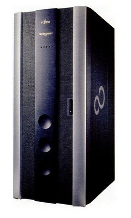
The Itanium was developed by Intel working together with Hewlett-Packard, which had agreed to use the Itanium as its successor to chips and systems based on the HP-UX architecture. Eventually, when Intel decided to discontinue the Itanium, this led to a lawsuit by Hewlett-Packard against Intel. Despite the Itanium being generally regarded as an ignominious failure for Intel, at the height of its success, systems based on the Itanium were made by a considerable number of companies. Shown at left is a Primequest server from Fujitsu.
The Intel i860 was more powerful than, and was introduced, in September 1989, later than, the Intel i960, despite the confusing numbering. This chip, like the Itanium, was designed to execute several instructions in parallel; as it also was not successful in the market, some have criticized Intel for failing to learn from experience in then proceeding with the somewhat similar Itanium. However, there were other grounds for viewing VLIW technology as being intrinsically promising, despite any failures in marketing or execution of any specific implementation of the technology. The i860, precisely because of its reliance on a deep pipeline to provide high speed, had the issue that when the pipeline was flushed by an interrupt, the resulting delay compromised performance.
One Intel i860-based workstation was the Neoware Supra-66, a thin client. Also, with appropriate workloads, pipeline delays on interrupts were less of an issue, and thus Intel's Paragon supercomputer, based on the i860, enjoyed some success at the time.
The Pentium Pro, from November 1, 1995, introduced Physical Address Extensions, so that x86-based systems could have large memories even if individual programs could only make use of a virtual memory no more than 2 gigabytes in size.
AMD responded by announcing their plan to provide a 64-bit extension to the x86 architecture in 1999. Their first 64-bit Opteron chips were released in April, 2003, and Intel accepted that 64-bit virtual addresses were needed by their x86 customers, and so they accepted the AMD scheme under their own name of EM64T (with a few minor changes; nearly all programs use the subset of features common to both manufacturers) releasing chips which used it starting from 2005.
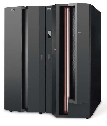
In the meantime, IBM delivered its first mainframes with the 64-bit zArchitecture, modified from the 32-bit architecture of previous mainframes derived from the IBM System/360, in 2000. The z990, the top-end machine in the first generation of System/z, is shown at right.
The z990 was built from multi-chip modules. In these modules, several dies contained one CPU each; however, they contained most of the components for two cores, because each instruction was executed in parallel twice, side by side on the halves of the chip, so that the results could be compared in order to provide an extremely low probability of errors. Going to such lengths, of course, would be considered wasteful by home computer users.
The current generation of zSystem is the IBM z16, introduced on April 5, 2022. It is the ninth generation of zSystem mainframes; the CPU chip used in it has a clock frequency of 5 GHz, and has eight cores on one die.
There were still a number of RAS features (Intel used that acronym to stand for Reliability, Availability, and Security, whereas originally IBM used it to mean Reliability, Availability, and Serviceability; of course, unlike an IBM 360 mainframe, one can't open up a microchip to swap out circuit boards) provided on Itanium processors that were not available even on the high-end commercial server Xeon chips with the x86 architecture.
This changed much later, in 2014, with the introduction of the Xeon E7 v2 line of processors.
October 12, 2011 was the day when the FX-4100, FX-6100, FX-8120 and FX-8150 processors from AMD were released. These were Opterons with four, six, and (in the last two cases) eight cores respectively, based on the new Bulldozer microarchitecture.
These chips were made on a 32nm process. A pair of cores shared a single 256-bit SIMD unit, which limited the design's power for programs that made use of AVX-256 instructions.
The base clock frequency of the FX-4100 was 3.6 GHz. However, the Bulldozer design was based on individual pipeline stages with a small number of gate delays, like that of the Pentium 4 from Intel.
It should be noted, though, that this is also true of the CPU chips inside current IBM mainframes. This type of design is workable in those IBM mainframes, although not for conventional desktop microcomputers, because IBM uses advanced water cooling in those mainframes. Shorter pipeline stages are not a bad thing; they provide more throughput, since more instructions can be executing concurrently within the pipeline (the pipeline being fed with instructions that don't each depend on the result of the immediately preceding instruction either by means of careful programming (facilitated by certain characteristics of RISC architectures, like their large banks of registers), or through out-of-order execution, or through simultaneous multi-threading (SMT)).
This was the beginning of a difficult era for AMD. Chips made with the Bulldozer microarchitecture, and its successors, Piledriver, Steamroller, and Excavator were percieved as having very disappointing performance. This led to AMD competing primarily in the lower end of the market, and having to price their chips based on the performance they achieved which was less than expected.
On March 2, 2017, the first Ryzen chips, the Ryzen 7 1800X, the Ryzen 7 1700X, and the Ryzen 7 1700, were available from AMD. These chips were based on an all-new Zen microarchitecture which corrected the mis-steps of the Bulldozer microarchitecture.
These chips were the first ones from AMD to include SMT (simultaneous multithreading), a feature Intel had offered for some time under the brand name HyperThreading.
Although the Zen microarchitecture was a big improvement over Bulldozer and Piledriver and the rest, however, the performance of an individual core was not equal to that of a single core on an Intel processor.
But the Ryzen processors from AMD were still very impressive, because they had eight cores, while Intel processors had four.
Intel did also make server processors with higher core counts, and indeed during the Bulldozer years, AMD also made Opterons with 12 and 16 cores. (The 16 core one was a Piledriver, however.) Those chips, being intended for business, sold at premium prices. So software intended for the consumer, particularly computer games, generally wasn't designed to make effective use of a larger number of cores.
Thus, Intel's competitive response to the introduction of the first Ryzen chips was to come out with a six-core chip, the i7-8700K in October. Because the individual cores were more powerful, it matched the eight-core Ryzen chips in total throughput, but because there was more performance in each core, it performed significantly better on games that could only make use of a limited number of cores.
This was widely percieved as Intel's way of indicating that it did not regard AMD's initial Ryzen chips as particularly impressive.
Also, while AMD placed a 256-bit vector unit in each core with Ryzen, rather than sharing them between cores as in Bulldozer and its related successors, Intel had increased the amount of vector processing power in its cores, leaving AMD still behind.
The next generation of AMD Ryzen chips was announced on August 13, 2018; these included significant improvements over the previous generation, but Intel had also been improving its processors.
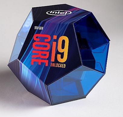
On October 8, 2018, Intel announced the i9-9900K processor, a top-of-the-line chip that was also unlocked to allow overclocking. It was referred to as the "World's Best Gaming Processor", and those who tested and reviewed the chip in the months following generally agreed that this was no idle boast, but the truth.
As befitted an impressive processor, it was initially sold in an impressive package, pictured at right from a publicity still included by Intel in the press kit for the announcement.
The chip had eight cores, and used Intel's HyperThreading technology, which meant that it provided sixteen threads. Its base clock frequency was 3.6 GHz; it could boost a single core up to 5.0 GHz for additional performance for limited periods of time, and it could also boost all or some of the cores by a lesser amount.
Providing faster boost clocks was a common feature of microprocessors at this time, and still is; it increases performance significantly because it helped with those portions of tasks that were compute-bound, which often were small enough that the boost clock could improve performance on most of them.
The third generation of AMD Ryzen chips was announced on July 7, 2019. At this point, AMD had achieved near-parity with Intel. AMD had spun off its physical chipmaking functions to a separate company, GlobalFoundries, in October, 2009. Because of the high cost of building facilities to make chips at more and more advanced process nodes, GlobalFoundries eventually declined to pursue the next major node after 14nm, although they have gone somewhat beyond that later with a 12nm process.
As a result, AMD was having the CPU portion of its Ryzen multi-chip module processor chips made by TSMC on their 7nm process. This was the earliest TSMC 7nm process, the one that did not involve EUV lithography at all in its production.
The computer which I used when originally composing these pages, and which I am still using even as I compose these very words, uses a processor from this series, the 12-core Ryzen 9 3900 (I was only planning to go 8-core, but that's what they happened to have on the day I walked in to buy a CPU). Thus, I have a different opinion than some people about the recent news in August of 2022 that SMIC in the People's Republic of China has not only managed to produce 7nm chips on a non-EUV process, but they're even selling them to the public in crypto mining rigs, instead of them only being used in secret military equipment; while this can still be dismissed as a dead end, not allowing further progress, I don't feel it can be dismissed on the basis that such chips aren't powerful or impressive.
Intel's 10nm process was basically equivalent the the process TSMC called 7nm, but Intel was having troubles getting it to work. Those troubles would turn out to take longer than expected to emerge from.
So with the third Ryzen generation, there was no real reason to hesitate in getting an AMD processor, if one wanted the best.
On November 5, 2020, AMD announced their fourth generation of chips. While the previous generation was close enough to Intel's chips in per-core performance that the difference was not significant, with this generation AMD could now claim leadership.
Meanwhile, Intel was finally able to produce chips in volume on its 10nm process. However, not all the problems with that process had been eliminated; they were only making laptop chips on the 10nm process, because they could not attain clock rates that would be competitive on the desktop with that process as it was.
Thus, on March 30, 2021, Intel released the i9-11900K and the i7-11700K, among other chips, based on the 14nm process. They were based on designs originally intended for 10nm chips.
Many reviews of these chips criticized them as having performance that was not much better, and perhaps even slightly worse, than their predecessors in Intel's previous generation.
However, these chips included support for AVX-512 instructions; and so I had suspected that when programs are written to make effective use of this new capability, they will turn out to be very impressive, thus giving AMD extremely serious competition. As of this writing, though, events have yet to justify my optimism.
Since the above was written, Intel has made it clear that AVX-512 was never really intended to be a feature of their 12th-generation Alder Lake chips (these are from the generation following the i9-11900K and i7-11700K mentioned above, these being 11th-generation Rocket Lake parts), and the ability to perform these instructions will be fused off on later production, so it was not intended to use this as a feature providing a competitive advantage over AMD on a continuing basis for the time being. In fairness, the fact that many of the chips in this line-up had both P-cores ane E-cores, with the E-cores not containing circuitry for AVX-512, would have made that feature awkward to use in any case.
More recent developments have included: AMD added AVX-512 support to its latest generation of CPUs, the Ryzen 7000 series based on the Zen 4 microarchitecture, but they did so by having the two halves of a 512-bit vector processed on different clock cycles, so AVX-512 support did not directly bring those chips any improvement in floating point power (Intel chips had to slow their clocks when an AVX-512 instruction was being executed; while this reduced the gains, since the clock was not slowed all the way down to half speed, there was still a net gain from being able to process twice as many floating-point numbers at once); Intel's latest generation of chips, the 13000 series, is generally acknowledged as having finally taken the performance crown away from AMD, reclaiming it for Intel.
Now, in 2024, naturally additional developments have taken place. AMD's latest generation of processors, the Ryzen 9000 series, based on the Zen 5 design, finally offer full-width AVX-512. Intel's Lunar Lake processors for laptops have dropped HyperThreading, as in that situation, the feature added more to power consumption than it added in performance.
Also present on this site is this page with a few words concerning recent events in the GPU rivalry between AMD and Nvidia.