How could the techniques reviewed on the previous pages be used to produce a computer with the kind of flexibility that I seek?
Many ways suggest themselves, including methods applicable to computer hardware conforming to present-day standards, with memory modules that provide 64 bits of data at a time to the processor.
However, if a different word size were to be found desirable, eventually, the available hardware would be changed to suit it.
The most compelling reason to consider word sizes different from the series of powers of two of bits, leading to a word of 32 bits or 64 bits, is that 36-bit floating-point might be usable where 32-bit floating-point is not, and thus in some cases 36 bits would do the work that now takes 64 bits.
Thus, the most simple and natural change would be to shift from memory modules that present 64 bits of data at a time to memory modules that present 72 bits of data at a time.
With 64 bits of data, the options of 64 bit or 72 bit memory modules are available, the latter allowing 8 bits for ECC; a code based on the Hamming code, plus a parity bit, is used in that case, providing single-error correction and double-error detection (SEC/DED).
With 72 bits of data, while a change is being made in the standard anyways, I would suggest that while the options of memory modules that are 72 bits wide, or 80 bits wide, to provide a SEC/DED error-correcting code, could be available, modules 88 bits wide should also be supported. This would allow the use of an error-correcting code based on the Bose-Chaudhuri-Hocquenghem (BCH) code, which, with 14 ECC bits, and one parity bit, provides double-error correction and triple-error detection (DEC/TED).
This takes up 87 bits, but the chips used in memory modules are 4 bits or 8 bits wide; having a 73rd bit available that can be used to tag a 72-bit doubleword, which could be used, for example, to flag permissible branch targets in executable code, seems to be potentially beneficial and therefore worthwhile.
Of course, ignoring one bit out of every nine isn't too terribly wasteful, so operating in a mode providing compatibility with the 64-bit computing world of today is also possible. If it is desired to use 36-bit floats from there, though, doubling the width of the memory bus, so that fitting seven 36-bit words into 252 of 256 bits is possible, would be desirable.
Incidentally, since 72 is three times 24, a possible drastic fallback mode, to permit operation, say, in high-radiation environments with larger rates of soft errors, suggests itself. One could use three 24-bit blocks of the Golay Code so as to store 36 bits of usable data in each 72 bit memory word under such adverse conditions.
Given the large number of pins on current microprocessors, a technique to permit the use of standard 64-bit wide memory parts is not impossible.
If one uses ten identical memory parts at a time, for a memory organized with two 320-bit wide data buses, each with its own address bus, then each data bus would contain 288 bits of data, 17 bits of DEC/TED BCH error-correcting code, and fifteen bits left over for possible use as tag bits. Since sixteen error-correcting bits can support up to 240 data bits, alternately one could use one sixteen-bit set of ECC bits to cover 112 bits of data in two of the memory parts, and another sixteen-bit set of ECC bits to cover 176 bits of data in the other three memory parts.
As outlined in a previous page, the simplest way to handle 48-bit and 60-bit floating-point numbers in a 36-bit architecture would be to embed them in a 72-bit double-precision floating-point number; they could be unpacked from, and packed to, a compact form when not in use.
Since 36 bits is a multiple of 12 bits, which is an appropriate basic unit for a computer with a 48-bit word, the technique outlined in the previous page could be easily applied to enable the computer to work with 48-bit data. More to the point, addressing the memory as a series of 12-bit units, on the boundaries of which 36-bit, 48-bit, and 60-bit data could all be placed, becomes fully straightforward, and so this would be a mode more suited to programs making frequent use of several of the different floating-point precisions I wish to support.
In addition, another well-established trick used on quite conventional computer systems to facilitate the handling of unaligned operands can be used so that when a 48-bit architecture is emulated, or 48-bit memory is provided, it can behave more like the "real thing", instead of being severely limited in the width of data items it can handle.
This technique is to have two memory buses, each with its own set of address lines as well as data lines. Even words are fetched from one bus, odd words from the other. This way, data items that straddle word boundaries, as long as they only straddle one such boundary, may be retrieved with a single fetch.
Thus, let us suppose that our processor chip can read and write 144 bits at a time, and that the data bus is divided into two 72-bit halves, each with its own address bus.
What will we be able to achieve with such a memory organization to provide a flexible environment with a 48-bit word? The diagram below will help to illustrate the possibilities.
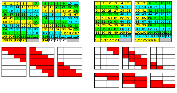
In the upper left of the diagram, we see how a group of consecutive 60-bit floating-point numbers could be stored within a single block of eleven 144-bit memory lines (each of two 72-bit memory words) used to contain 32 architectural words each 48 bits in size.
Since 60 bits is equal to five memory units of 12 bits each, despite the fact that at the end of the block, 48 bits out of the 72 bits available in each memory word are used, as five is only one more than four (the number of 12-bit memory units in 48 bits), only one memory word boundary can be straddled.
The bottom half of the diagram shows how no possible position of either a 60-bit float or a 36-bit float, with alignment on 12-bit boundaries, will straddle more than one memory word boundary.
If we're providing a 48-bit word design, what about 96-bit extended precision?
That can also be supported, provided that operands of this side are aligned on 96-bit boundaries. The upper right portion of the diagram reminds us that the last eight 12-bit memory units in the block, where a problem is likely to arise, constitute a single 96-bit item aligned on a 96-bit boundary, since the block provides 128 memory units.
This neat fit, of course, doesn't apply to the 72-bit double-precision float format of the parent architecture. So are we stumped?
No! It is true that six is two more than four. However, three is only one more than two. So, since 72 is three times 24, all that needs to be done is to require that 72-bit floating-point numbers be aligned on 24-bit boundaries, and they too can be handled with ease.
The trick is that instead of just taking 32 consecutive 48 bit words, and putting them in the first 32 positions of 33 consecutive 48 bit words in 11 memory lines of 144 (3*48) bits, some additional logic is used so that the last 96 bits are split in half between the two memory banks.
That way, the empty space at the end doesn't reduce the minimum width of a contiguous stretch of data within one of the memory banks below 48 bits, which is what allows the successful handling of 60-bit and 72-bit floats in all cases.
The main concern of the scheme is to avoid the need for a division by three. So one instead uses a shift to divide the address of a 48-bit word in the simulated 48-bit wide memory by 32, with the quotient indicating which block of eleven 144-bit memory lines is used. Multiplication by 11, unlike division by an odd number, is simple.
The sequence of addresses in the diagram, though, within a single block, seems to require special handling of the last line. Without such special handling, though, a division by three applied to the last five bits of the address is the operation needed to locate data within the block.
So, the special handling is not a problem because that last step in address conversion would be done using a table in order for it to be done very quickly. Thus, any arrangement is possible, even if it could not be achieved with simple logic.
Thus, instead of making the minimum width of data in either half-memory 48 bits, the minimum could have been held to 60 bits by having 24 bits of unused space in each of the last two rows. But that would not have provided a real benefit.
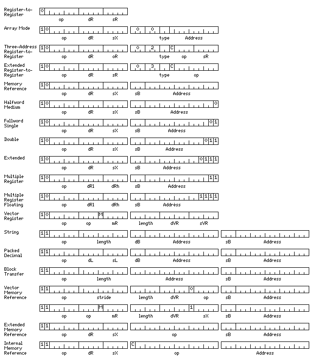
A possible instruction set layout for a computer with this memory layout is illustrated below:
The register complement provided would be:
As is apparent from the diagram, the instruction formats strongly resemble those of the IBM System/360, but there are important differences, some involving taking advantage of the 36 bit word length.
There are sets of eight base registers, separate from the 32 arithmetic/index registers used for fixed-point numbers.
One set is used for normal data in the native memory treated as 36/72/144 bits wide. The alternate base registers are instead used for those instructions that deal with instructions dealing with data that appears to be in 24/48/96 bit wide memory.
The alternate base registers contain addresses that still refer to a 9-bit character in normal width memory. But it is the sum of displacement field in the instruction and the index value, if any, that is an address referring to a 12-bit storage unit in the simulated 24/48/96 bit memory, converted by the techniques above to access the data within the actual 144 bit wide memory lines.
This compromises between converting only the index value, on the one hand, as against going to the other extreme of allocating blocks of simulated 24/48/96 bit memory through the operating system.
While the instructions are of variable length, the proportion of instructions that are two basic units in length (here, 36 bits long, twice 18 bits; on the System/360, 32 bits long, twice 16 bits) was reduced from one-half of the opcode space to one-fourth; just as the number of registers is increased to 32, as found in RISC machines, the memory-reference instructions will be limited to load/store instructions.
Since normal memory is organized in 9-bit characters, but alternate width memory is organized in 12-bit memory units, and 12, unlike 9, is a multiple of 4, the packed decimal instructions which follow the System/360 pattern of being variable-width memory-to-memory instructions will use alternate width memory. That is, if such instructions are even provided, since their usefulness is questionable on contemporary machines where external DRAM is very slow compared to the computational speed of the processor. However, cache memories have proven themselves effective in covering a multitude of sins, so I do not wish to be absolutely categorical about this.
Considerable effort is needed to free up more opcode space, since there will be instructions for all the following data types:
The memory-reference instructions for the first eight data types listed would use the normal base registers, and those for the last seven data types listed would use the alternate base registers, and addresses would be in units of 12 bits instead of 9 bits.
Thus, the fact that in some cases, aligned operands will have unused bits at the end of the displacement field has been used to allow the same opcode to be shared between different instructions. (As I've noted elsewhere on this site, this technique was used with the SEL 32 minicomputer from Systems Engineering Laboratories.)
The data types listed above are the ones provided as a basic feature of the computer's normal mode of operation; in addition, as noted above, it would presumably be provided with the capability of operating as a computer with a 32-bit word length; here, 32 bits of data would simply be placed in each 36 bit word, without taking any further elaborate steps to improve the efficiency of storage use.
Further thought has led me to think that the complexities of simulating 24/48-bit memory could be avoided, while still providing a full selection of the desirable floating-point data types.
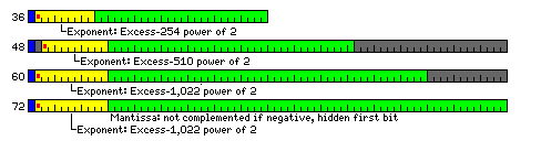
Instead of attempting to provide a 60-bit floating-point format, an alternate 72-bit floating-point format with a reduced precision could be provided by allocating 17 bits instead of 11 to the exponent field.
This would, however, lead to a further departure of this design from the IEEE 754 standard, since now the extended precision format would have to have a longer exponent field; I propose that 23 bits be allocated for the exponent, in a 108-bit extended precision floating-point format, to make it a superset of all the available types.
Is there enough room for all the opcodes that would be needed?
If one allocates 16 basic opcodes to each integer data type, and 8 basic opcodes to each floating-point data type, as there are six integer data types, and seven floating-point data types (since distinct register-to-register instructions are not needed for floating-point numbers of the same length, but stored in 48-bit memory as opposed to 36-bit memory), 152 opcodes are needed for register-to-register instructions. Only 128 opcodes are actually available for them; plus, an additional 16 opcodes would be desirable for unnormalized operations on the two extended precision data types.
Since memory-reference instructions are of the load/store type, each integer type only requires four operations (Load, Store, Insert, and Load Unsigned), while each floating-point type only requires Load and Store. This makes for a total of 40 opcodes, out of a total of 64 available opcodes, and here some opcodes will be shared, further reducing those required.
The following types could share opcodes:
16 bit halfword, 32 bit integer
24 bit integer, 48 bit integer
54 bit intermediate precision, 36 bit floating point, 72 bit double precision, 144 bit extended precision
72 bit double precision in alternate memory, 48 bit intermediate precision, 96 bit extended precision
thus, effectively, for memory-reference instructions, there are four integer data types and four floating-point data types, so that only 24 opcodes are needed.
Rather than attempting to make do with only 8 opcodes for things like load and store multiple instructions, branch instructions, and shifts, so that an additional 32 opcodes could be switched from indicating 36-bit instructions to indicating 18-bit instructions, it would be perhaps preferable to follow the practice IBM used when extending the System/360 instruction set, and allow some register-to-register instructions to take up 32 bits rather than 16 bits, causing them to occupy only a negligible part of the opcode space.
However, the two rarest types - 36-bit and 72-bit floats in the alternate memory space - have already been eliminated completely. Extended precision, of both the 144 and 96 bit kind, and 72-bit long integers are possible candidates.
Alternatively, however, allocating 192 opcodes to 18-bit instructions, and 32 opcodes to each of 36-bit and 54-bit instructions is a possibility that should not be overlooked. If, for example, only even-numbered registers could be used as index registers, it would be possible to provide an extra opcode bit to turn 32 opcodes into 64 opcodes once again for most of the 36-bit instructions, although that wouldn't work with the load multiple and store multiple instructions.
If stride is not used, the memory-reference vector instructions already have four unused bits, and they're load/store instructions. But the register to register vector instructions would appear to need a considerable amount of opcode space, so they might have to be shifted to being 54-bit instructions.
However, further reflection turned up some additional possibilities, and so the split of 128/64/64 opcodes by length, instead of going to 192/32/32, can be retained.
The register-to-register vector instructions also have four free bits that can be used as part of the opcode.
When the index register field contains zero, that means indexing is not present. On the System/360, a base register field containing zero also meant that base register contents were not added, leading to absolute addressing, which was normally little used.
One option for using this value would be to indicate "array mode", a form of indirect addressing which allows a program to access a number of large arrays without having to dedicate a base register to each one. But a table of 1,024 array addresses seems adequate, and so other modes can be made available as well. Originally, 32,768 addresses would have been the starting point, decreased to 4,096 by using three bits to specify a mode, but an additional two bits are required because the same opcode could be a load instruction for up to four different data types, since opcode space is being conserved by using the least significant bits of the address to distinguish between types where they would otherwise be wasted in the case where all operands are aligned.
Given that the hardware has the capability of supporting unaligned operands, as that capability is required for the variable sizes of data being supported, this suggests that 54-bit versions of the memory-reference instructions that don't impose an alignment restriction should also be provided; and, of course, this would use only a negligible amount of opcode space.
So, for the load instruction for each data type, a 36-bit register-to-register instruction with additional opcode bits could be indicated by following a zero in the base register field with an octal 3 in the next three bits. This format could be used for register packed decimal instructions, for example, which are far more practical than memory-to-memory packed decimal instructions under current conditions where memory accesses are very slow compared to processor speeds, especially in terms of latency.
For a given type, four bits are needed for the standard operations; as well, another two bits would be dedicated to disambiguating the different data types of related lengths that might be distinguished by the least significant bits of the displacement field for memory-reference instructions. As no extra bits are left for the opcode field in the case of a three-operand instruction, a two-operand 36-bit register-to-register instruction is also shown, to allow additional operations to be made available. Note that a bit is included to indicate if the condition codes are to be updated by the instruction. This makes it possible to avoid having a conditional branch instruction depending on the immediately preceding instruction. It also implies that the 18-bit register-to-register instructions do not affect the condition codes.
One way of making use of an internal memory is provided; the 54-bit memory-reference instructions include an alternative form where an 18-bit address, this time an address in units of 9 bit characters, replaces the base and displacement fields for normal memory reference. Since the internal memory is intended to be much faster than external memory, instructions that perform arithmetic operations from operands there would not compromise efficiency, and so the condition code update bit is included in that instruction format as well.
It is envisaged that when program instructions are fetched from that internal memory, the address constant portion of the 36-bit memory-reference instructions will be changed to be an 18-bit address of an internal location, while the 54-bit memory-reference instructions (other than instructions such as the string instructions, which will also change) will continue to provide access to both internal and external memory.
Access to memory organized with a 32-bit word instead of a 36-bit word is not described here; that is something needed for intercommunication between native mode and emulation programs as opposed to being part of the normal arithmetic capabilities to be provided for routine operation, so handling it via a mode bit, an instruction prefix of some sort, or some related technique seems fully adequate.
The instructions that are 36 bits long, with the bits 10 as their prefix include both the basic memory-reference instructions, and alternate forms of the register-to-register instructions, so those instructions alone would be sufficient for a complete RISC instruction set.
The prefix bits, then, would be available for reuse to indicate when instructions depend on one another, and when instructions can't be executed at the same time due to a resource conflict. While the former case may require a delay up to a pipeline flush, the latter only means the instruction must be started in the next cycle.
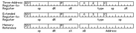
Here, a third bit is made available by allowing only the even-numbered registers to serve as destination registers. This means that a register-to-register form of the store instruction is required.
The bit marked D indicates an instruction that depends on another instruction; the bit marked Y indicates a cycle break, that is, when instructions need to be started on the next cycle because an ALU is used again as was previously used, and the bit marked P indicates the instruction that is depended upon. Having both the D and P bit means that a complete pipeline flush can be avoided, since the cycles taken by the intervening instructions can be taken into account.
Decreasing the size of the destination register field can be avoided, and some additional information can be provided with an instruction block format like the following:
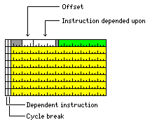
Instructions are in blocks of eight. When going from one block to the next, there would always be an implied cycle break, so the first cycle break bit would be unused. For compatibility purposes, it should always be set to 1 rather than 0 as would be the usual practice with an unused bit; this way, a future implementation might fetch and execute multiple blocks at once.
The first instruction slot in a block contains the eight bits indicating which instructions are depended upon; in addition, there is a four bit field indicating if any additional P bits are set between a D bit that is set, and the set P bit in the instruction on which the instruction with the D bit depends.
But there is still an instruction in the first instruction slot - just an 18-bit register-to-register instruction instead of a 36-bit instruction.
One issue is that it might seem preferable to put the instruction position with the extra information and the shorter instruction in the last position, instead of the first one, because at the beginning of a program, the registers need to be filled with data from memory before register-to-register calculations can begin. But this design is described as having memory buses with a total width of 144 bits; although a larger implementation could have a 288 bit bus, it is desired not to make that mandatory. Therefore, the additional information has to be available within the first 144 bits of the block.
Many of today's popular RISC architectures use 32 registers. And many of these architectures have out-of-order implementations.
The features characteristic of current RISC designs, particularly load/store memory-reference instructions and a larger number of registers than found on conventional computer architectures, are relevant to avoiding the need to incur the cost of out-of-order execution.
Instead of shifting groups of instructions that use the same registers to execute in parallel, but on different registers, when possible, if a large number of registers is available, the compiler can, explicitly, in advance, interleave the sequences of instructions for multiple calculations that can execute independently.
Either way, the computer is doing useful work while waiting for instructions on which later instructions depend to complete their execution in the pipeline.
But the total number of registers available limits how many sequences of instructions can be interleaved; this is why RISC architectures now have out-of-order implementations, because as processor makers have sought ever-improved performance, the number of pipeline stages used for execution has increased. If one has to allow seven cycles between dependent instructions, having only four sequences of instructions to interleave, which allows three other instructions to be placed in between, is not enough.
A technique to increase the number of available registers without adding bits to the instructions makes use of the fact that the large number of registers is being used primarily to interleave sequences of instructions, each sequence individually only needing a relatively small number of registers. Thus, if one has a destination register field and a source register field that are both five bits long, they can be replaced by a destination register field that is seven bits long and a source register field that is three bits long. Both fields refer to a register from the same set of 128 registers (unless, of course, one of them refers to a floating-point register), and the first four bits of the destination register field are prepended to the contents of the source register field to determine the source register to be used.
This does, however, compartmentalize the 128 registers into 16 groups of 8 registers, which limits flexibility.
Thus, I present a modified version of this technique:
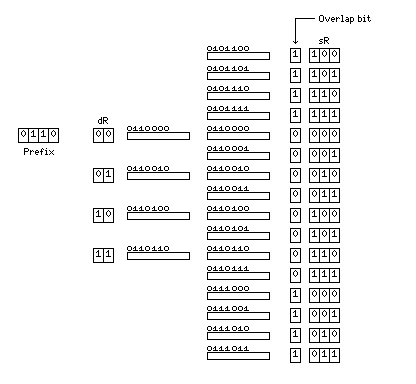
Here, the first four bits of the destination register field are still the prefix which is shared with the source register field.
But an extra bit is added to the source register field, an overlap bit. If that bit is set, the last four of the eight registers specified by the last three bits of the source register bit are moved to the group of eight registers preceding the one indicated by the prefix bits; the first four of those eight registers are moved to the group of eight registers following the ones indicated by the prefix bits. (The set of 128 registers does wrap around for this purpose.)
To make this extra bit available, while still having 128 registers in use, only even-numbered registers are allowed to be used as destination registers. Thus, a register-to-register store instruction is now required as well as the register-to-register load instruction.
Thus, as illustrated in the diagram above, there are sixteen groups of four destination registers; each of these groups of destination registers can interact with sixteen possible source registers, and each possible source register can interact with two such groups of destination registers.
In addition to destination registers, index register fields and operand register fields are changed to this four-bit form, so in a three-address instruction there is now one unused bit. In the case of an index register field, the bit patterns 0000 and 1000 will both indicate that indexing will not take place, so that register 0 in any group of 8 registers is never used as an index register.
Some register fields are not changed in this mode: the index register field in a vector memory-reference instruction, and the mask register fields in vector instructions, both register and memory-reference. In 128 register mode, the bits 10 are appended at the end of the contents of these fields, to use registers 2 and 6 within each group of 8 registers.
As for the load multiple and store multiple instructions, these cannot be usefully adapted; instead, 54-bit load multiple and store multiple instructions, with room for two 7-bit register fields, are required.
Although in describing an example ISA, we have gone on to addressing other questions, the initial rationale for the design was to change the selection of floating-point precisions offered to the programmer. Does that in fact serve a purpose?
In my opinion, the best way to assess that is to review the number of terms that can be added with a Wallace Tree adder based on its number of stages:
 0     2
 1     3
 2     4
 3     6
 4     9
 5    13
 6    19
 7    28
 8    42
 9    63
10    94
11   141
12   211
The number of bits in the mantissas of the different floating point formats to be made available are shown below:
Size   Mantissa  +1   /2   Stages  Adder

36-bit based formats
 36          26  27   14     6       5
 54          43  44   22     7       6
 72          60  61   31     8       6
144         128 128   64    10       7

24-bit based formats
 36          26  27   14     6       5
 48          37  38   19     6       6
 60          48  49   25     7       6
 72          60  61   31     8       6
 96          80  80   40     8       7

Standard 32-bit based IEEE 754 formats
 32          23  24   12     5       5
 64          52  53   27     7       6
128         112 112   56     9       7
First, we start by looking at how many bits are used for the mantissa in each size of floating-point number. Then we add one for the hidden first bit, except for the extended formats which do not have that.
Then we divide by two, rounding up, because Booth encoding halves the number of partial product terms needed.
Finally, from our earlier table of values, we can see how many stages deep our Wallace Tree needs to be.
Thus, it turns out that the 32-bit floating-point formats fare very well in terms of efficiency, offering the highest precision of those listed for the number of Wallace Tree stages they use.
However, 96-bit extended precision, and 48-bit intermediate precision, also offer efficient use of two additional depths of Wallace Tree.
What I view as significant, though, is not so much achieving maximum efficiency as establishing that most of the formats offered have some reason for existence. 36-bit floats actually do offer less latency than 64-bit floats, so they're worth using when they can be used to avoid the need for double precision.
Of course, the multiplier output then feeds an adder related to a Sklansky adder, and so here the significant sequence is that of the powers of two. So the final column shows the number of adder stages the different formats require, and that does provide additional differentiation between the different formats.
Aside from considerations of efficiency, however, there is another thing to consider. A 48-bit float offers 11 decimal digits of precision; a 54-bit float offers 13 decimal digits of precision.
Desktop scientific programmable calculators, and the pocket calculators that succeeded them, displayed numbers with 10 digits of precision and a two-digit exponent, which suggests this is the ideal precision for general scientific and engineering work when one can freely choose what precision to use. However, calculators that displayed 10 digits of precision tended to have additional precision internally to ensure that the results they displayed would not be visibly inaccurate.
Some calculators had only one extra digit of precision, and some had as many as five extra digits. Both the early Texas Instruments scientific calculators and the NORC had three more than ten digits of precision, corresponding to the precision offered by a 54-bit floating-point number.
With this as an argument that 54 bits is better than 48 bits, then, a pure 36-bit architecture without additional facilities for simulating 48-bit wide memory might well be a better choice, since both 36 bit floats and 54 bit floats belong to the 36-bit realm.