In the previous section, we looked at taking the opportunity posed by a switch to more robust error correction to also widen memory from 64 bits to 72 bits.
But if one stays more realistic, it is possible to move from a SEC-DED code to a DEC-TED code for memory organized around the 64-bit word without using special memory parts. 112 data bits require 15 check bits for a double-error-correcting BCH code. 239 data bits require only one more bit, 16 check bits, for a double-error-correcting BCH code.
U.S. Patent 4,509,172, granted on April 2, 1985 to IBM, specifies a DEC-TED-S4ED error-correcting code; in addition to correcting double errors and detecting triple errors, it also detects the failure of a four-bit-wide memory chip. (The patent shows two versions of the code; the first version applies to nine-bit-wide memory chips instead.)
This code required only 16 check bits to protect 128 data bits.
This is despite the fact that a Bose-Chaudhuri-Hocquenghem code with 15 check bits can only provide double error correction for 112 data bits, and requires a 16th check bit giving overall parity to also provide triple error detection. Apparently, BCH codes are not optimal, or it may simply be that adding triple error detection to a code that provides double error correction is easier than adding double error detection to the Hamming codes which provide single error correction, and no longer requires adding a full bit to the code.
In that case, while an efficient DEC code can be directly constructed by the BCH technique, an efficient DEC-TED code requires code shortening to be done.
So if we support unaligned memory addresses by having two address buses and two data buses, now each data bus is 128 bits wide, and so we can access 256 bits of memory in a single operation.
And that means we can handle 36-bit floating-point numbers with little waste, following the scheme that has been described several times elsewhere on these pages. Seven of them would occupy 242 bits.
A block of five memory words could be used as the basic unit; of the 35 36-bit units it would contain, the last three could be left unused.
Unfortunately, it isn't possible to find a multiple of seven that is just one more than a power of two; that's because seven is 111 in binary; that issue was discussed at greater length on this page.
But 48 is just one less than 49; however, it is three times sixteen, and so using it as the basic unit would still involve a division by three. But using, for example, two blocks of 48 plus one block of 32 to make a larger block of 128 would reduce the percentage of waste and not require as large a lookup table as would be needed for going to the next size of block with three unused spaces, a block of 256 items out of 259 in 37 memory units of 256 bits. So there may be possible workarounds worth considering.
One could also use ten blocks of 48 plus one block of 32 to make a larger block of 512.
As before, instructions that reference 36-bit floats would have their addressing handled as follows: they would use an alternate set of base registers which contain conventional addresses aligned on a 256-bit boundary, and the sum of the displacement in the instruction and the index register contents (if indexing is used) would be converted from a 36-bit address in order to locate the memory operand of the instruction.
The last two bits of the address could be used to indicate a nine-bit byte, so as to maintain a full analogy to the conventional addressing of the machine.
48-bit floating-point numbers can be stored, aligned on halfword boundaries, in conventional memory with a 64-bit unit. Given that the memory bus is designed to support unaligned data, the only assist that is needed to make handling such data efficient is an alternate indexing mode where only the index register contents are modified during addressing, and the modification would simply include a multiplication by three, which is just a shift and add.
A shorter 96-bit form of extended precision floating-point numbers can also be supported in this way, and so could 24-bit integers, although there may not be enough opcode space to permit the attempt.
Given that nine is 1001 in binary, just as three is 11 in binary, it might be asked why not handle 36-bit numbers the same way as 48-bit numbers: multiply a 36-bit unit address by nine to get a nybble address, which can easily be used to find the correct part of conventional memory, with no wastage. There are two reasons why this choice was rejected, even though indeed the dual-bus arrangement, with its power to enable the handling of unaligned data, can facilitate this as well as bit addressing. The first reason may seem trivial: conventional addresses are by the byte, rather than the nybble, and so unlike the case of halfword-aligned 48-bit values, some additional special handling over and above multiplying the index by nine is required. The second reason is that while 16 bits is a relatively coarse subdivision of memory, a 4-bit nybble is a sufficiently fine subdivision that the better part of a barrel shifter would be required to facilitate this mode. On the other hand, when seven 36-bit numbers are placed in a 256-bit memory unit with four bits left over, they are in the same positions in every 256-bit memory unit, and so only wiring, and not shifting, is required. |
It would certainly be possible, if desired, to divide 255 of the 256 bits in a memory word into five 51-bit floating-point numbers. Then, a group of thirteen such memory words would contain 65 such numbers, of which only 64 could be used for ease of addressing.
What about using the memory organized in 36-bit units for 72-bit double-precision numbers, or 54-bit intermediate precision numbers?
By ensuring that the last four 36-bit units in a block of thirty-two are evenly divided between the two halves of the 256-bit data bus, as shown in the diagram below,
the support for unaligned operands which having two 128-bit data buses, each with their own address bus, provides is indeed sufficient to ensure that such operands could never straddle three 128-bit memory units.
Although I think at this time that support for 51-bit floats is not important enough to justify adding a third view of memory, particularly when a 48-bit view of memory can be fully supported with ease, and I do not view adding 72-bit double precision as all that useful (except, of course, as an assist in emulating a computer with a 36-bit word length), I am strongly tempted by 54-bit floating-point numbers, because they provide a useful amount of extra precision, compared to 48-bit floats, when accuracy to ten decimal digits is desired from a computation.
If 51-bit floats were also handled, then they could be stored like this:
As it happens, 51 is not a prime number, it is 3 times 17. But that would mean another layer of address conversion to make thirds of these items addressable to allow processing of 34 or 68 bit data items, should that be desired for some reason. So 51-bit data units are lacking in versatility, compared to 36-bit data units.
Aside from being an approximation to a 48-bit float with three extra bits of precision, one could also fit a sign and fifteen decimal digits with Chen-Ho encoding in a 51-bit unit.
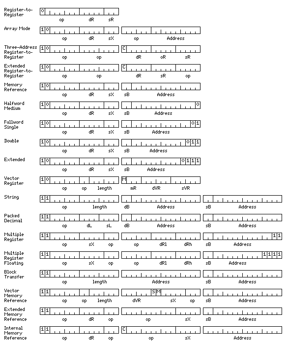
A possible instruction set layout for a computer with this memory layout is illustrated below:
The register complement provided would be:
This is the register complement from the viewpoint of the programmer.
For VLIW mode, the number of available arithmetic/index registers and of available floating-point registers may each be increased to 512.
As well, as it is envisaged that the processor would be capable of multithreading, there would be several copies of the complete set of registers, with the exception of the 64 vector registers. Long vector processing, patterned after what the Cray I and other vector supercomputers provided, would not necessarily be available to every thread, but perhaps only to one or two threads.
In order to keep the processor as busy with code in the conventional instruction format as it is intended to be possible with the 512-register versio of VLIW mode, the ability to handle at least 16 threads concurrently, with instructions from eight of those threads starting execution simultaneously in each cycle, is required.
This allows an implementation to have the characteristics needed to run VLIW code at full speed: eight-way superscalar capability, even in some cases where the data types of the instructions to be executed are not diverse, and a pipeline depth such that eight cycles may often be needed from one instruction to the first one that depends on its result. This assumes well-written RISC code in each thread such that, usually, in each thread there are four instructions from one instruction to the first one that depends on its result, around which the division of the 32 registers in each of the two principal sets into four groups of eight is designed.
Incidentally, note that this implies that the maximum superscalar ability of such an implementation will be more than eight ways, so that it would be useful to have an even higher level of multithreading, such as 32 threads, to take advantage of the opportunity to execute instructions dealing with different types of data. Even the ability to handle 128 concurrent threads would be helpful, to allow the design to cope with code that does not consist preponderantly of sequences which interleave four calculations at once; in this way, throughput would at least be maintained even when all the available threads consist of code in which each instruction depends on the immediately preceding one. (However, this is not the worst case; it is still required for maximum throughput that all the code running does most of its calculations in registers, with only infrequent accesses to main memory - although it's only the cache misses that need to be really infrequent.)
Note that this implies the number of cores per die is likely to be limited to one, since each thread will need a certain amount of bandwidth to main memory, whether the threads are all on the same core or split between multiple cores with a smaller multithreading capability.
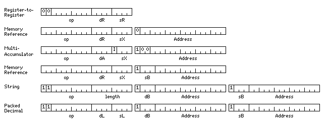
As is apparent from the diagram, the instruction formats strongly resemble those of the IBM System/360, but there are important differences.
There are two sets of four base registers, separate from the 32 arithmetic/index registers used for fixed-point numbers.
One set is used for normal data in the native memory treated as 32/64/128 bits wide. The alternate base registers are instead used for those instructions that deal with instructions dealing with data that appears to be in 36 bit wide memory. Not only are 54-bit floats not supported, 72-bit enlarged double precision is also not supported.
The alternate base registers contain addresses that still refer to an 8-bit character in normal width memory. But it is the sum of displacement field in the instruction and the index value, if any, that is an address referring to a 9-bit character in the simulated 36 bit memory.
This compromises between converting only the index value, on the one hand, as against going to the other extreme of allocating blocks of simulated 36 bit memory through the operating system.
While the instructions are of variable length, the proportion of instructions that are 32 bits long was reduced from one-half of the opcode space to one-fourth; just as the number of registers is increased to 32, as found in RISC machines, the memory-reference instructions will be limited to load/store instructions.
Some effort is needed to free up more opcode space, since there will be instructions for these following data types:
The alternate base registers would only be used to address 36-bit floating-point numbers from among the types shown above. While 9-bit characters, and 18-bit and 36-bit integers could also be supported using the alternate base registers, unlike 36-bit floats, they are not urgently needed.
The fact that in some cases, aligned operands will have unused bits at the end of the displacement field has been used to allow the same opcode to be shared between different instructions, in order to conserve opcode space. (As I've noted elsewhere on this site, this technique was used with the SEL 32 minicomputer from Systems Engineering Laboratories.)
Although I envisage having sixteen short vector registers, each 256 bits in length, and using those registers also for a bit matrix multiply instruction, I have not attempted at this time to include the formats of the related instructions in the table above.
It is intended to make such instructions available as 32-bit instructions if possible, so that they can be used in VLIW mode.
The 16-bit register to register instructions do not affect the condition codes; if it is desired to affect them, a 32-bit register to register instruction, which has a C bit that, as on several RISC architectures, indicates the instruction is to affect the condition codes if it is a 1, must be used.
Is there enough room for all the opcodes that would be needed?
For register-to-register instructions, what is needed is:
16 opcodes each for four integer types and for two extended precision types; 16 times 6 is 96.
8 opcodes each for four regular (always normalized) floating-point types: a total of 32.
So that uses up all the 128 available opcodes allocated to 16-bit instructions. That is unfortunate, but acceptable: there would still be some spares, as the sets of instructions won't need to be a full eight or sixteen instructions in all cases, and no other categories of instruction are 16 bits long.
As well, this calculation assumed that a full complement of unnormalized arithmetic instructions would be provided for both 96-bit and 128-bit extended precision numbers in 16-bit form. In fact, however, those are instructions of sufficiently low priority that it is more reasonable to only provide them among the register-to-register instructions in 32-bit form, for which more opcode space is available.
For memory-reference instructions, the situation is more complicated.
For integer types, in general four instructions are needed for a load-store instruction repertoire: load, store, insert, and unsigned load.
But only 8-bit characters take a set of opcodes to themselves.
A second set of opcodes would handle 16-bit halfwords, 32-bit integers, and 64-bit long integers.
For floating-point types, only load and store are required.
48-bit intermediate, 32-bit, 64-bit, and 128-bit floats can all share one set of opcodes.
36-bit floats, though, would be separate, and so would 96-bit floats.
But 48-bit and 96-bit floats with alternate indexing could share a set of opcodes.
The regular 48-bit intermediates could be grouped with the 96-bit floats as well.
So in total, the requirement is for two sets of four opcodes, and four sets of two opcodes. This totals to sixteen opcodes, and there are 64 opcodes available for 32-bit instructions.
Only four base registers, instead of eight, are used, and so other opcodes are used for array mode and 32-bit register-to-register instructions with this architecture, unlike the 36-bit architecture which preceded it.
For vector register instructions, the three-bit mask register field indicates one of registers 2, 6, 10, 14, 18, 22, 26, or 30 as being the mask register, if the M bit is set.
For the vector memory reference instructions, if the five-bit index register field contains any value with the last three bits all zero, indexing does not take place.
The S bit indicates that stride is present; the stride value is taken from register 1, 9, 17, or 25, depending on the first two bits of the index register field.
The M bit indicates a bitmask is used to select elements of the vector that will be operated on; the mask value is taken from register 2, 10, 18, or 26, depending on the first two bits of the index register field.
The instructions that are 32 bits long, with the bits 10 as their prefix include both the basic memory-reference instructions, and alternate forms of the register-to-register instructions, so those instructions alone would be sufficient for a complete RISC instruction set.
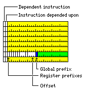
The prefix bits, then, would be available for reuse to indicate when instructions depend on one another, and when instructions can't be executed at the same time due to a resource conflict. While the former case may require a delay up to a pipeline flush, the latter only means the instruction must be started in the next cycle.
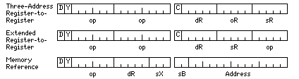
Here, a third bit is made available by allowing only the even-numbered registers to serve as destination registers. This means that a register-to-register form of the store instruction is required.
The bit marked D indicates an instruction that depends on another instruction; the bit marked Y indicates a cycle break, that is, when instructions need to be started on the next cycle because an ALU is used again as was previously used, and the corresponding bit in the group of eight bits in the second-last instruction slot indicates the instruction that is depended upon. Having both the D and P bit means that a complete pipeline flush can be avoided, since the cycles taken by the intervening instructions can be taken into account.
Decreasing the size of the destination register field can be avoided, and some additional information can be provided with an instruction block format like the following:
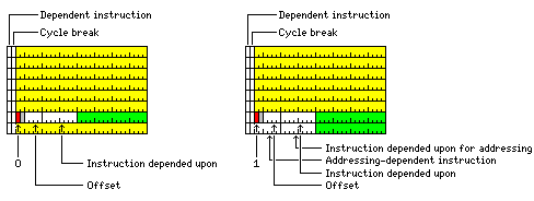
Instructions are in blocks of eight. When going from one block to the next, there would always be an implied cycle break, so the first cycle break bit would be unused. For compatibility purposes, it should always be set to 1 rather than 0 as would be the usual practice with an unused bit; this way, a future implementation might fetch and execute multiple blocks at once.
The second-last instruction slot in a block contains the eight bits indicating which instructions are depended upon; in addition, there is a four bit field indicating if any additional P bits are set between a D bit that is set, and the set P bit in the instruction on which the instruction with the D bit depends.
But there is still an instruction in the last instruction slot - just a 16-bit register-to-register instruction instead of a 32-bit instruction.
Here, the special instruction slot is at the end, instead of at the start, since we have a full 256-bit data bus (required to accomodate 36-bit data) rather than possibly only a 144-bit data bus, so there is no need to put that instruction slot in the first half of the block. However, it is in the second-last slot, instead of the last one, to allow a 32-bit conditional transfer instruction to be placed in the last slot, thus reducing the need for NOP instructions.
The diagram shows that there are two possible formats for the VLIW block.
In the second format, shown on the right, the last instruction slot also contains only a 16-bit instruction, making room for two additional fields of supplementary information.
The six-bit field refers only to the first six instructions in the block, as they are 32-bit instructions which may be memory-reference instructions.
The dependent instruction bit indicates that an instruction depends on a previous instruction for one of its source operands. Even when that bit is set, the contents of the index register and the base register that the instruction may use are assumed to be available, so that address calculation can be done well in advance of the main portion of instruction execution.
So the six-bit field indicates for those first six instruction slots that an address calculation dependency does exist.
The following eight-bit field indicates the instruction depended upon for those instructions.
No offset field is provided for these dependencies. It is assumed that the need to explicitly indicate such dependencies will be rare, because usually ordinary dependencies will take precedence. Thus, given four instructions, A, B, C, and D, which occur in that order, with other instructions possibly between them, if instruction C depends on instruction B, that takes precedence over instruction D also depending on instruction A (normally; instruction A might take much longer to complete than instruction B), and not all instruction dependencies are indicated, only those necessary to avoid dependency hazards.
Because the instruction lengths are 16, 32, and 48 bits, rather than 18, 36, and 54 bits, the shortest instructions already share two bits of the destination register field with the source register field. Therefore, going from 32 registers to 128 registers in the fashion described for the 36-bit architecture that inspired this one would not work for those instructions.
However, having only 32 registers is a serious problem for the VLIW mode of operation at least.
The intent of the VLIW mode is that the eight instructions fetched in a block of instructions are normally not only independent, but also cause no resource conflicts, so that they can all be simultaneously issued in a single cycle.
And then the eight instructions in the next block will not only be independent of each other, but they will also be independent of the ones in the block before, so that they can all be simultaneously issued in the next cycle.
But with thirty-two registers, divided into four groups of eight, what is facilitated is having four calculations going on at the same time, where usually the next instruction in the same calculation is dependent on the one before in that calculation.
Assuming a modern implementation with about, say, 12 stages in the pipeline, if, to make a round number, we assume that only eight of those stages are execute stages... we still need, now, for the VLIW mode to work properly, to have sixty-four calculations going on at once, all interleaved, so that we can fill eight blocks of eight instructions before having to come around again to an instruction that depends on the result of one of the eight instructions in the first of those blocks.
One can't perform sixty-four concurrent calculations with thirty-two registers.
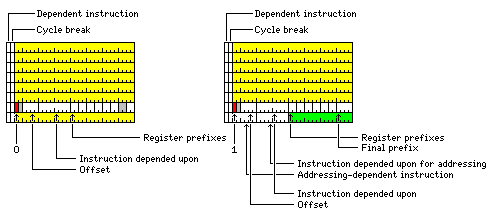
Here is a modified format for the instruction block that allows more registers to be used in a simple brute-force fashion:
The 16-bit instruction in the second-last instruction slot is removed, and replaced by a set of two-bit fields, one for each of the other instruction slots, that indicates which of four banks of 32 registers is used for the corresponding instruction.
Thus, 128 registers are available within each block of eight instruction slots; these blocks now only hold seven instructions; one of them can be a 16-bit instruction in the case where an addressing dependency is indicated.
The two bits which correspond to the second-last instruction slot are used as a further prefix, selecting which of four banks of 128 registers is used for the given block.
The sequences of bits which indicate dependencies between instructions are now divided into four streams, each stream pertaining to those instruction blocks which use one of the four banks of 128 registers.
Since 32 registers already support four ongoing calculations, and that is multiplied by four when going to 128 registers, and by four again when going to 512 registers, it now is possible to have eight instruction blocks (containing up to 56 instructions) with no dependencies present.
Of course, while it is possible to keep the processor well-utilized with code expressed in this fashion, not every problem can be broken up into that many streams of calculation that can also be positioned statically relative to each other. Which is why this VLIW mode is not the machine's only mode of operation, and why it is envisaged as being able to support a large number of simultaneous threads.
While the 512-register VLIW mode created the theoretical possibility of fully utilizing the processor power with a single thread, as noted, this will likely only be achievable in special cases. Signal processor applications are likely to be among those cases, as VLIW is used with DSP chips.
The one unused bit in the diagram of the block format could be used to switch the positions of the two sets of prefix bits; this would allow a ninth block to contain the one 'missing' instruction from the previous eight blocks, now limited to seven instead of eight instructions, so that there could be 63 independent instructions in a row instead of 56.
Note that since the 32-bit instructions do use five-bit register fields without shared bits, a technique similar to the previous 128-register mode could be used in addition in order to achieve a 2,048-register mode of operation if necessary; in that case, though, the 16-bit instruction slot available when addressing dependencies are indicated will likely be unusable.
However, while that many registers appears to be excessive, one can still modify the formats of the 32-bit instructions in that fashion:
and simply not use the global two-bit prefix, just using the two-bit individual prefixes to indicate which of four banks of 128 registers is used for each instruction. Thus, while the number of registers is still 512, now any of those registers, not just those from a single 128 register bank, are available within a single block of eight instruction slots.
In this case, the destination register for register to register instructions can be any of the 128 available registers, not only the 64 even-numbered ones, as with the previous 128-register mode. In the extended two-address register instruction, the source register must be in the same group of eight registers as the destination register chosen. In the three-address register instructions, the same technique as used in the previous 128-register mode is used to allow the use of the last four registers in the previous group of eight registers or the first four registers in the next group of eight registers:
0000   current  000
0001   current  001
0010   current  010
0011   current  011
0100   current  100
0101   current  101
0110   current  110
0111   current  111
1000   next     000
1001   next     001
1010   next     010
1011   next     011
1100   previous 100
1101   previous 101
1110   previous 110
1111   previous 111
In the case of memory-reference instructions, the five bit destination register field is padded with two zeroes on the right to identify one of registers 0, 4, 8, 12... 124. The index register field is either 0, to indicate no indexing, or indicates a register from 1 to 7 within the same group of eight registers as the destination register field indicates.
And, finally, because this is now a flexible 512-register mode instead of a 2,048-register mode, the problem of the 16-bit instruction when addressing dependencies are indicated is solved. Instead of leaving the two bits formerly used for a global prefix unused, they can be combined with the two existing prefix bits for the last instruction slot to give it a four-bit prefix, so the instruction format, referencing a bank of 32 registers, does not have to be modified for access to 512 registers.
Thus, the format of a VLIW instruction block becomes that shown in the diagram above.
Some aspects of VLIW mode can be discussed in more detail as we examine how it can be made more efficient.
If the extent to which the design is superscalar is subject to change from one model of the chip to another, this would mean that the values to put in the cycle break field would also change.
Unlike dependencies, though, it is fairly simple to determine from the opcode of an instruction which ALUs it would use. So that field could be dropped as unnecessary, and so the bit indicating the instruction depended on could be put in the second bit position.
Why was a separate set of bits added to indicate addressing dependencies?
The thinking behind that was that the contents of the index and base registers would be used at an earlier stage in the processing of an instruction than the contents of the source register field.
So an addressing dependency between two instructions separated more widely than two instructions with a normal dependency that are closer together could still be the one more likely to cause a conflict. But if that is the case, there is no need to nest both dependencies, only the more serious one needs to be noted.
However, a load instruction can only have an addressing dependency (excluding dependencies involving the memory location referenced, as opposed to the registers used), and so it's only a store instruction that can have both types of dependency.
Which one is present can be resolved from which register is modified by the instruction on which it is dependent.
So it seems as though one can also drop the separate indication of addressing dependencies.
With those steps taken, there is now enough room to include a one-bit prefix for each instruction, with a three-bit prefix for the 16-bit instruction, to allow access to 256 registers.
Because 16-bit instructions always start with a zero, there is one last bit still available, which can be used as a global prefix, and so we can still have a 512-register mode.
So now we have a 512-register mode with eight instructions in a block, not just seven, and only one instruction being a 16-bit instruction instead of a 32-bit instruction. Since the global prefix is only one bit long instead of two, it offers more flexibility than the original attempt at a 512-register mode, although less than the more flexible version.
However, if one needs more than eight cycles before an instruction can depend on the result of a preceding instruction without causing a stall, that means that more than 64 independent instructions in a row need to be possible. And that means that there need to be some independent instructions that both share the same group of eight registers.
It should be possible to manage to find a few, so that one could go for, say, ten cycles, one block choosing eight of the first thirty-two sets of eight registers, and the second block choosing eight of the second thirty-two sets of eight registers. And that would stretch things enough to cover current levels of pipelining, before an extension to even more registers would have to be considered.
The other alternative is simply to accept that even with 512-register VLIW mode, two threads in that mode would have to be running to keep the chip busy.
If we are going to the trouble of creating a 512-register mode so that the VLIW mode has the possibility of performing to expectations, at one block of instructions per cycle, then is the bit indicating a cycle break still necessary?
After all, that bit indicates that more than one instruction is seeking to use the same ALU. If the chip isn't superscalar enough to handle eight instructions at once, why bother with VLIW mode?
Originally, the answer was obvious enough. There would be one add/subtract unit, one multiply unit, and one divide unit, for each size of operand. So, as there are are more than two sizes of integer data, and more than two sizes of floating-point data, it would be possible to keep the computer busy; but the cycle break bit would still be needed because many types of problem mostly involve just one size of data.
Given the desire for the highest possible performance, though, that view of the design may be modified somewhat: for the most favored data types, extra ALUs may be provided. I am thinking that it would not at all be inappropriate to have eight add/subtract units and eight multiply units for 64-bit floating-point, even if one would still just have only one divide unit.
Thus, the cycle break bit is still clearly needed, since the same provision is not made for all data types, but a high level of performance is provided for what is seen as the case where the maximum performance is most seriously needed.
The other question has to do with the provision of an addressing mode that accesses data in a 64 kilobyte area of internal storage.
Will that be a temporary dedicated area taken from cache, or will it be an additional area without the overhead of being able to act as cache?
64 kilobytes is not that much, so presumably several such areas could be provided, one per thread.
But that's still a lot of storage to save and restore in external DRAM if that were needed; and if that is not going to be done, how is the allocation of what still is a limited resource to be managed?
And, more importantly, how useful is it?
While it is only shown in the instruction formats overview as being accessed from 48-bit memory-reference instructions, I envisage its primary use to be from within VLIW mode, where three mode bits replace all memory accesses of one (or perhaps more) of the three possible types (regular data, 36-bit data, program code) with accesses to the internal memory.
Then it does become clearer what the internal memory is useful for: unlike cache, in addition to providing speed, it provides predictability. All the memory accesses from within such a VLIW program, not just almost all of them, will take place quickly.
In addition, this internal memory may be multiported, with one write port but eight read ports. This would allow it to be connected to a set of ALUs that allow the evaluation of a formula involving several variables to be started in every cycle. This is another way in which a performance increase might be enabled.
Given the requirement for a five-bit field indicating the index register, and a four-bit field for the condition, a 32-bit conditional branch instruction will take up two opcodes. That, in itself, is not a problem.
In VLIW mode, where all dependencies are explicitly specified, normally a branch will require the pipeline to be flushed. However, for loops, the need to do this can be avoided by unrolling loops as follows: the first iteration stands by itself outside the loop which contains the rest of the iterations.
In this way, as long as there are no dependencies that go back beyond the previous iteration, while the dependency bits in the first iteration will refer to the code that preceded the loop, dependency bits in the remaining iterations will be able to refer equally well to the iteration preceding the loop or the previous iteration of the loop.
Since instructions that are depended on are indicated by flag bits attached to the instructions themselves, and they are not pointed to by relative pointers, it is not needed to terminate the first iteration with a dummy instruction (say the NOP formed by a branch on no condition without flushing instruction) in order to ensure a correct alignment of dependency targets.
In any case, this means that for use within VLIW mode, two forms of the conditional branch instruction need to be provided, the normal one and a special non-flushing one used at the end of loops to branch back for a repetition.
In addition to loops formatted in this way, a non-flushing branch is also appropriate where the branch, if taken, is not into a sequence of code where there is code before the branch point which can also fall through into the target, but instead where the branch chooses between two forks, neither of which is entered from any code except that preceding the branch instruction.
Further thought has led me to conclude that there is a way to go to 36 bits with standard memory parts.
Just have three 64-bit data buses, each with its own address bus, coming from the chip. Then inexpensive 64-bit DRAM modules could be used.
If 16 bits are reserved for one tag bit, 15 error-correcting code bits (14 BCH, one parity), then one has 3 times 48, or 144, bits of data - which is twice 72 and four times 36.
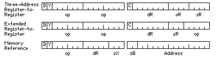
Instead of going to the architecture of the previous section, I'm now thinking in terms of these instruction formats:
The machine would have 16 general registers, 16 floating-point registers, 8 base registers, and 128 index registers.
Base registers 0 and 1 would serve a special purpose.
Base register 0 would point to a 32 kilobyte region which corresponds to scratchpad memory. This region would have to be aligned on a 32 kilobyte boundary. It would be cached directly to a special L1 cache which would be, as it could be due to that alignment restriction, direct-mapped.
Base register 1 would point to a 128 kilobyte region which would serve as the primary memory window of programs, allowing a large linear address space.
The other base registers, from 2 through 7, would point to normal-sized segments, each 16 kilobytes in size.
Normally, the 16 general registers would also serve as index registers for memory-reference instructions.
But in the multi-accumulator mode, where the region indicated by base register 0 is used, the index register field would be reduced to three bits, to select one of seven index registers (or no indexing, if 0) associated with each of the sixteen general registers.
With a separate set of base registers, none of the general registers has a special meaning attached, so all sixteen can be used as accumulators, and compilers can with relative ease directly indicate in the generated code a high degree of instruction-level parallelism (ILP) by interleaving up to sixteen programs which would be very similar to programs on an old-fashioned machine with a single-address memory-accumulator architecture.
In addition to limiting things to 128 index registers instead of 256, reducing the size of the index register field in this format allows room for an indirect bit; so indirection is usually from this L1 cache, basically viewed as an extension of the complement of registers, and this provides what I have referred to as "array mode"; the addresses of many arrays can be stored here, allowing many very large arrays to be used without needing to dedicate a base register to each one.
By having sixteen general registers, and not trying for 32, the opcode field can be enlarged, and so there should be no problem with allowing a large number of data types.
The ability to access memory as if it were organized in 48-bit words, however, would be less important, although it might still be useful to handle six-bit character data.
The floating-point data types I would support would be:
Name                        Length    Alignment
Single Precision             36 bits   36 bits
Intermediate Precision       54 bits   18 bits
Double Precision             63 bits    9 bits
Classic Double Precision     72 bits   72 bits
Extended Precision          108 bits   36 bits
Full Extended Precision     144 bits  144 bits
their formats being as shown in the diagram below:
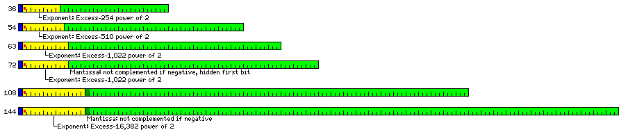
All these types could be fetched from DRAM with a single access, as given the alignment shown, they could not span more than three consecutive 48-bit data elements. This is despite the inherent wastefulness caused by 48 bits not being a multiple of the basic 9 bit unit. However, because the DRAM is split into three parts, not two, while most unaligned fetches avoid a penalty, this is not true for the 144-bit Full Extended Precision data type, which must be fully aligned on a 144-bit boundary to avoid the need to fetch twice from the same DRAM stack.
Being so bold as to add a byte-aligned floating-point type allows one to closely approach the common 64-bit double-precision floating-point type, but with a small reduction in precision.
Thus, my original goals are met:
Single precision is increased to 36 bits, giving precision comparable to that of the IBM 7090, plus exponent range comparable to that of the IBM 360, thanks to the IEEE 754 hidden bit.
Intermediate precision, at 54 bits, is an improvement on my original objective of 48 bits, as a data type corresponding to the 10-digit precision of pocket calculators, but now with three extra digits to help ensure calculations can yield a full 10 digits of precision in their final result, instead of just one extra digit.
Double precision, at 63 bits, now replaces my original objective of 60 bits. This was chosen on the basis that the Control Data 6600 provided adequate precision for scientific calculations, while 64-bit floating-point numbers were excessive. The exponent field in IEEE 754 floats is the same size as that used on the Control Data 6600, and, as well, the hidden first bit means the mantissa has an additional bit of precision. So 60 bits would have been fully satisfactory; while 63 bits is therefore not really an improvement, the fact that it comes closer to what 64 bits offers means that it is even less likely that it will be necessary to resort to 72 bits.
However, I realized that I overlooked one thing. If my intention is not to have a CISC architecture that is dependent on out-of-order execution in order to run efficiently, then I need to follow the example of most RISC architectures, and have some way of dealing with conditional branches properly: such as by including a bit to indicate whether an instruction will set the condition codes.
That leads to this:
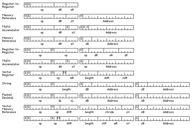
The memory-reference instructions and the register-to-register instructions now have the same number of bits in the opcode field, so it still isn't necessary to overlap memory-reference opcodes by allowing only aligned operands.
This gives an opcode field that is one bit longer for the multi-accumulator instructions, allowing opcodes for additional specialized operations.
Since three-address register-to-register instructions have space for a five-bit register field, using sixteen of a complement of 32 registers of each type for the normal general registers, and the other sixteen as the accumulators suggests itself.
To allow the string and packed decimal instructions access to the workspace memory, and to allow the workspace address to be loaded without the need for a special dedicated register, though, there would still be space for workspace instructions starting with 01 instead of 10, since base registers 0 and 1 would remain both dedicated to a special purpose as described above. Should this opcode space be dedicated to special instructions, or some new, exotic address mode? Another possibility, as shown above, would be to allow workspace instructions using the regular general registers instead of the accumulators as their accumulator; both would share the same set of index registers for a given value in the destination accumulator field.