In this section, we've examined several approaches to endowing a computer with the ability to conveniently handle data with several different sizes which are not simple power-of-two multiples of one another.
First, we considered the possibility of using a small unit, of which the lengths of all the types of data with which we were concerned were mutiples. This had the obvious problem that a wide bus to memory allows memory to work considerably faster.
Second, we considered using a bus to memory that was wide enough that each type of data with which we were concerned would fit on that bus an integer number of times. Aside from the problem that a 720-bit bus was wide enough to be impractical, which was addressed by using only a 120-bit bus instead, this had the problem that converting logical addresses of some types of data to physical addresses in this type of memory required division by three or by five. While a circuit can easily perform multiplication by three or five by a shift and add, to my knowledge, division can't be simplified to that extent, which would be a hindrance to working with arrays of values in widths other than the ones most natural to the system.
Third, a scheme was examined that would allow address conversion to be simple and rapid for all the sizes of data that would be used. But it brought with it one subtle performance problem: while fetching 192 bits from memory would bring four consecutive 48-bit values to the computer, consecutive 36-bit values or consecutive 60-bit values, at least when they were organized so that they could be easily addressed as part of an array, would be in consecutive 192-bit memory words. This would reduce memory bandwidth and consume space in Level 2 cache.
Also, in another section of these pages, concerned with an illustrative computer architecture, I discuss a scheme for allowing the use of variable-width items in memory that involves using the Level 2 cache. The cache is presumed to be organized in cache lines consisting of sixteen memory words, where the size of a memory word is a power-of-two number of bits, and data items of variant sizes are accessed through the cache by partially filling cache lines. Thus, if 36-bit words are used, nine of the sixteen memory word positions in a cache line are used; if 48-bit words are used, twelve of the sixteen memory word positions are used, and if 60-bit words are used, fifteen of the sixteen memory word positions are used. Addressing avoids the divide-by-three problem, as only multiplication is required to obtain physical addresses.
Is there any possibility that this situation can be addressed in a fashion that avoids the flaws of the approaches described above?
One other scheme that hasn't been covered yet indeed does avoid the problems noted above. It does have a problem of its own, which may be a relatively minor problem in comparison: it requires the use of a significant number of extra pins on the socket of the microprocessor involved.
Incidentally, the name of this scheme was inspired by an IBM laptop with an expanding keyboard, and the similarity of the scheme proposed here to an idea I had for a display screen which could alternate between 4:3 and widescreen aspect ratios.
A computer could handle 36-bit, 48-bit, and 64-bit data efficiently through the following scheme:
Provide the processor with two separate 32-bit data buses to main memory, each of which has its own address bus as well.
Memory mapping logic inside the processor could make it appear to the processor that it had arbitrary amounts of 36-bit wide memory, 48-bit wide memory, and 64-bit wide memory connected to it as follows:
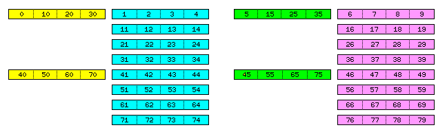
A 64-bit wide data item could be fetched with one 32-bit half being located in one memory bank, and the other 32-bit half being located in the other memory bank.
Successive 48-bit wide data items could have their first 16 bits located in both halves of the 32-bit memory words obtained from one memory bank, and their remaining 32 bits stored in the memory words of the other memory bank.
Successive 36-bit wide data items could have their first 4 bits located eight to a 32-bit memory word in one memory bank, and their remaining 32 bits stored in the memory words of the other memory bank.
If, in addition, one has the option of using either of the two memory banks for the small part of a data item which is stored two or eight to a memory word, while the other one stores a full 32 bits of a data item, then the two memory banks can be equal in size and efficiently store an arbitrary mix of data of each of the possible sizes.
This does have the limitation that data items belonging to the different size families could not be intermixed in close proximity while still taking advantage of the efficiencies which this design offers. Presumably, for input-output operations, direct memory access would deal with memory exclusively as though it were composed of 64 bit words, and memory-mapped I/O devices would also be in address space that would have to be treated in this fashion, and so if binary data of an alternative length is to be placed in a data structure for I/O purposes, it would have to be copied into 64-bit address space out of 36-bit or 48-bit address space. Given the inherent slowness of I/O operations, however, this would be an inefficiency that would be a small price to pay.
Incidentally, while each block allocated would have to have the small part of an odd-length data item consistently in one of the memory banks, in order for the blocks to have power-of-two lengths, allocating blocks in pairs of opposite handedness, and having memory addresses interleaved between them, such as by having 36-bit words allocated as eight to one block and then eight to the other block, might be useful to avoid a reduction in data bus bandwidth that still does arise in this scheme due to the data path to the bank with multiple partial words per memory word being less used. Of course, the bandwidth of the address bus is still halved.
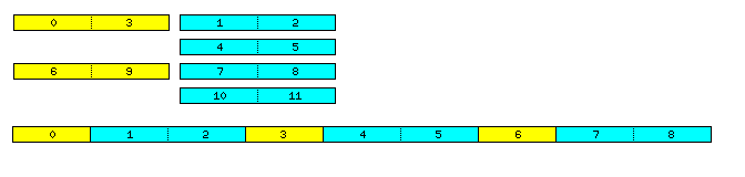
This image shows the principle of how alternating the memory bank containing the small parts of words could be used to maintain full use of memory bandwidth from both banks, given a sufficient prefetch of consecutive words:
The illustration happens to show the assembly of 40 bit words instead of 36 bit or 48 bit words. Also, it ignores such details as the fact that conventional memory parts are 64 bits wide and not 32 bits wide, and the importance of fetching multiple consecutive words at a time for maximum efficiency with modern DDR3 memory, and so, in practice, interleaving would involve alternation between left and right after a larger number of words.
Incidentally, the only reason two address buses, each controlling half of the data bus, are required are in order to allow the fetching, in a single memory cycle, of an alternate-length word. If that is not required, and it is only required that full memory bandwidth is utilized for fetches of multiple sequential words to fill the cache, a single conventional address bus and data bus will do just fine.
However, with a single address and data bus, it is already true that if the hardware can handle unaligned data, then two memory accesses will be enough to fetch an item in memory of a nonstandard length which is only as much longer than a memory word as one unit of its alignment level; thus, with a 32-bit word, a 40-bit item aligned on byte boundaries cannot have the single byte by which it exceeds 32 bits extend outwards on both sides of the word. Thus, the benefits of this scheme as opposed to more conventional memory access appear to be quite limited in the case of a single bus.
Also, questions arise of how best to organize Level 2 cache for a computer of this design. Should each of the three size spaces have its own Level 2 cache? Or should the cache contain memory images, but with the two 32-bit wide memory banks being cached separately?
While the lengths of the blocks allocated are three or five times a power of two, this does not mean that the divide-by-three and divide-by-five problems are present, since dealing with such block lengths, if multiple small consecutive blocks were used for some reason, involves multiplying by three or five; this method applies to the case where it is the alignment problem, not the addressing problem, that needs to be dealt with.
Also, note that this works for such word lengths as 36, 40, and 48 bits because the binary representations of those numbers are 100100, 101000, and 110000, in each case with only two ones in the number. 60 bit words, since 60 is 111100 in binary, would take four memory banks to assemble using this principle.
Also, note that having two data buses with independent address buses, if the data bus is as wide as the widest data item of interest, eliminates the penalty associated with fetching unaligned data. Thus, if the data buses are both 64-bits in width, 48-bit data items (which could still be aligned on 16-bit boundaries) and 40-bit data items aligned on byte boundaries could be freely used, as, if they cross the boundary of a 128-bit area in memory, they could still be retrieved in a single memory cycle by using an address for the left memory bank that is one greater than the one used for the right memory bank.
In fact, the limit is actually one unit of alignment greater than the size of the data bus; thus, an 80-bit unit, aligned on 16-bit boundaries, could always be fetched in a single operation, as the 16 bits by which it exceeds 64 bits in width could not extend across three aligned 64-bit words in memory, only two. So a 72-bit unit aligned on 8-bit boundaries would also be fetchable in a single operation, thus achieving compatibility with 36-bit words without having to involve memory mapping.
Somewhat later, I took inspiration from another IBM computer, the IBM 7030 or the STRETCH, to come up with a version of this idea that would be adapted to a computer designed around with a different width of memory word.
The IBM STRETCH had a 64-bit wide data bus. Up to sixteen memory units, each containing 16,384 words, could be attached to the computer. Groups of two memory units could be accessed using two-way interleaving, and groups of four memory units could be accessed using four-way interleaving. A typical configuration involved attaching six memory units to the CPU. The first four, accessed using four-way interleaving, would be primarily used for data, and the last two, accessed using two-way interleaving, would be primarily used for program instructions.
This provided balanced performance, since typically the computer would access data twice as often, or more, than it accessed instructions.
Of course, the STRETCH still had a single data bus and a single address bus.
However, if a processor had two address buses, one governing a 64-bit data bus, and another governing a 128-bit data bus, and memory modules were installed in matched sets of three, then if it had, say, 6 gigabytes of RAM, a bit could be chopped off the first 4 gigabytes, and a bit half as large chopped off the last 2 gigabytes, to form an area of 192-bit wide data.
While normally this architecture would not be able to handle unaligned data without the possibility of some additional delay in the 8/16/32/64-bit wide series, it would be able to handle unaligned data in the 12/24/48/96-bit wide series, at least up to widths around 72 bits, and thus it would be suitable for handling 36-bit and 60-bit floating-point data types.
If it was necessary to process unaligned data in the 8/16/32/64-bit series, however, memory could be allocated in a way in which that would be permitted. First, allocate twice as many 64-bit words on the 64-bit side as 128-bit words are allocated on the 128-bit side. Only one of those 64-bit words can be between two successive 128-bit words (as is the case when 192-bit units are used) to allow unaligned data crossing the boundary on either side to be handled through accesses to the two different data banks; therefore, the other 64-bit word would need to contain data located within (ideally, in the middle of) the 128-bit word, so as to lengthen it to 192 bits.
This would allow data up to 72 bits in length to be aligned on 8 bit boundaries, the same as could be achieved with two 64-bit data buses.
But then this, of course, reveals how a similar thing might be accomplished in a design which is not built around the peculiar indulgence of a 48-bit word length. And, thus, I re-invented the idea I had already described on this page, but it led to my examining it more closely.
Starting with the case where a chip has two address buses, each one governing a data bus which is 64 bits, or 128 bits, in width - both data buses being the same width in this case - so that the second data bus is simply there for the primary and obvious purpose of allowing access to unaligned quantities belonging to the mainstream 8/16/32/64 bit series of widths.
If memory were to be allocated so that twice as many locations on one data bus were included in a block as were included on the other data bus, that would provide for data in the 12/24/48/96 bit series of widths. But, as noted above, if that series of widths were to be used for 36-bit and 60-bit floating-point numbers, then the ability to handle unaligned data is crucial.
Incidentally, it might be noted that I am well aware that today's DRAM chips are internally interleaved, and thus they are most efficiently accessed to provide data from blocks of consecutive locations. However, they still also allow it to be specified which element of the block will be presented first, so as to reduce the latency of fetches to a specific desired location in memory; and so the techniques I am describing here for unaligned accesses still serve to minimize the latency of fetching the complete word which happens to straddle a memory word boundary.
Let us assume the two data buses are each 128 bits in width. And let us represent a 192-bit memory line by the letters ABCDEF where each letter represents 64 bits of the data in that memory line.
On the side where memory is accessed at half the rate, let the data contained in one 128-bit memory word be AD.
On the side where memory is accessed more quickly, let the two consecutive words accessed contain BC and EF respectively.
Then data on the AB boundary is in AD and BC; data on the CD boundary is in AD and BC as well; data on the DE boundary is in AD and EF, and finally data on the boundary between the F of one 192-bit memory line and the A of the next memory line is in the next AD combined with the former EF. Thus, no boundary is between two consecutive locations on the same data bus, and unaligned data, in this case of up to 72 bits in length and aligned on 12 bit boundaries, is properly handled.
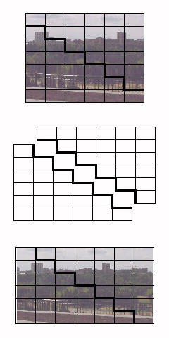
The diagram below:
illustrates how this works.
In the top section of the diagram, we see the order in which data is placed in the memory connected to the two data buses, with the one accessed at the slower rate shown in yellow, and the one accessed twice as often in cyan.
Below, the order in which this data appears in 192-bit organized memory as seen by the program is shown, and in each case, where two numbered areas in cyan are adjacent, they belong to the same 128-bit memory word; the other crossings are between yellow and cyan, where having two separate address buses mean that any two memory words may be brought together at those boundaries.
Thus, data items that are 64 bits long (and, in fact, slightly longer, depending on the granularity of alignment even for unaligned data), as they can't possibly straddle three of the numbered areas, are always accessible in their entirety in a single fetch.
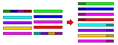
And, of course, needless to say, the pattern
 0  1     2  5
 3  4
 6  7     8 11
 9 10
works just as well as the
 0  3     1  2
          4  5
 6  9     7  8
         10 11
scheme which was shown, so the two memory banks can remain equally populated, even if the mix of memory used is light on the 32/64 bit series of widths and heavy on the 24/48 bit series of widths.
In examining the use of the Butterfly Memory concept, I encountered one difficulty. If the ratio between the pieces obtained from the two data buses is high enough, the length of data items that can be accessed in an unaligned fashion is governed by the shorter piece that is fetched.
The solution I came up with is to split each data bus into two halves, and then apply the Butterfly Memory principle to change the width of data separately in each half. In that way, the length of unaligned data is governed by half of the total length instead of by the shorter piece.
But since I use the two halves together for fetching unaligned data, I need only give each half the ability to fetch aligned data of the new width. This means I don't need four full address buses, instead I can use most of the address lines for the two parts of one half, with only two different versions of a small number of the bits of the address bus.
Just as three is one plus two, five is one plus four. So could this technique be used to handle memory aligned on units of ten bits as well?
One thing this would be useful for is dealing with data in Chen-Ho encoding, as this way the ten bits into which three digits are efficiently encoded would be the fundamental unit of memory, so that strings of digits the length of which is any multiple of three could be handled.
It certainly can be applied, but one problem arises if it is applied in the simplest and most straightforward manner.
Let us say that we take single lines of memory on one 128-bit data bus, and groups of four lines of memory on the other 128-bit data bus.
Then, each single line of 128 bits on the first side needs to be split into four parts of 32 bits each to permit the maximum length of unaligned data to be handled.
This lets us fetch, in a single operation, any of those 32-bit parts and either the preceding, or the following, 128-bit memory line on the other side, using the other data bus. But not both of them.
So one can fetch aligned data of up to 160 bits in length, but unaligned data, which may start at any 10-bit boundary, can only be up to 40 bits in length to always be possible to fetch in a single cycle.
This prevents putting 60-bit floating-point numbers in the 10-bit organized memory, they could only be in the 12-bit organized memory, which might seem strange.
The most obvious way around this would be to double the size of the two data buses. So instead of having two address buses, each of which controls a 128-bit wide data bus, there would still be two address buses, but each one would have a 256-bit data bus associated with it. This would also increase performance.
Well, this might work for the higher-performance versions of a given architecture intended to provide this feature.
But since it would doubtless be desired to offer chips in a range of performance levels and prices, it would be desirable to have another solution.
Another idea that suggests itself would be to have four address buses. So two address buses, each controlling a 64-bit data bus, would fetch an aligned 80-bit word from one side, and the other two address buses, each controlling a 64-bit data bus, would fetch an aligned 80-bit word from the other side, which could be the one preceding or following the first 80-bit word, thus allowing unaligned data of up to 90 bits in length.
However, four address buses is quite a bit of extra overhead. So that's not a particularly desirable solution either.
But there may be a way out.
With 128-bit data buses on each side, the only reason two full address buses are needed to fetch unaligned 64-bit data items is because they might start at address 000...01111111111111100 and continue to address 000...10000000000000000 so that many lines of the address would have to be changed.
If one is fetching only aligned data, one doesn't need a second full address bus.
But how will this work if we're using a memory system designed for 32-bit, 64-bit, 128-bit and so on, memory items for 40-bit and 80-bit data - or even 24-bit and 48-bit data - since we are going through half the memory four times or two times as fast, this means the addresses will still be quite different.
Here is a scheme which involves using only four extra address lines in each of the two full address buses.
External physical addresses, even on a system with 64-bit virtual addresses, might be 48 bits long, or slightly less, on a current microprocessor.
Let us suppose that for 8-bit series data, four block sizes are possible; 4K bytes, 64K bytes, 1M bytes, and 16M bytes. (Compare the three block sizes, 8K bytes, 64K bytes, and 512K bytes, offered on some Alpha processors.)
Since instead of single bytes, normally memory lines 256 bits in width are addressed, containing 32 bytes, the last five address lines are only used for partial-width accesses - not within DRAM, where the byte-select lines are used, but to I/O peripherals designed for a less-wide data bus also attached to the least significant lines of the data bus.
So the next seven bits in front of those last five complete a 12-bit byte address, enough to select a 4K byte block of memory.
Take the four address lines in front of those, and provide pins on the microprocessor package for two different versions of those lines, each routed to one of the two sets of 64-bit wide DRAM modules that populate one of the two 128-bit halves of the primary data bus with its own full set of address lines.
Well, sixteen is one more than fifteen, and fifteen is divisible by both three and five.
So one has a single 4K byte of conventionally-organized memory to allocate to some process whenever one allocated 60K bytes of memory as an area to be treated as built around a 10-bit unit. In the four address bits that are independent on the two halves, the first half of the block would use 0, 1, and 2 on one side, and 0, 1, 2, 3, 4, 5, 6, 7, 8, 9, A, B on the other; the second half would use 3, 4, 5, 6, 7, 8, 9, A, B, C, D, E on the one side, and C, D, E on the other, and so one has the ability to use three times as much memory in one half as on the other, then reversing halfway. 60K bytes would contain 48K 10-bit memory units.
Thus, it would work like this: each 128-bit side of the memory bus would supply one aligned 80-bit unit of memory at a time, alternating with 80-bit units of memory supplied by the other side of the memory bus, so that the fact that addresses on the two sides are independent would allow unaligned data to be accessed since each 80-bit unit could be read in association with either the one that precedes it or the one that follows it.
Thus, the first 320 bits in such a block would consist of 8-bit bytes from the following physical addresses, offset from the beginning of the block in physical memory:
00000 - 00001 16 bits
00008 - 0000F 64 bits
00010 - 00011 16 bits
00018 - 0001F 64 bits
00002 - 00003 16 bits
10008 - 1000F 64 bits
00012 - 00013 16 bits
10018 - 1001F 64 bits
Thus, the order in which pairs of bytes are used to create 80-bit units is illustrated by this diagram:
but in this case, the two columns which are filled, as they provide 64 bits out of every 80, instead of only a quarter as much, 16 bits, instead of showing consecutive 64-bit memory lines, show corresponding ones in successive blocks of 4K bytes of total overall memory, or 1K bytes, and hence 64K 64-bit memory lines, in the column itself.
So with this addition, we obtain a design with the following capabilities of memory allocation:
8-bit unit
 4K    64K     1M     16M

12-bit unit
    8K     32K     2M


10-bit unit
       48K
Memory organized around the 12-bit unit would be allocated in groups of three conventional memory blocks, and being limited in both granularity and size by the limits for conventional blocks, there would be three sizes instead of four. Memory organized around 10-bit units would only be allocated in one block size, dictated by the particular choice of address lines to duplicate between the two halves of each side of the memory bus.
However, there is one drawback, although I think it is minor. If one divides each 128-bit data bus into half, then if one is using ECC memory, it is no longer possible, in those pages which contain memory organized according to the 10-bit unit, to use a single 16-bit error-correcting code block to protect 128 bits of data according to a double error correcting and triple error detecting code (DEC-TED), but instead 8 error correcting bits must correct 64 bits of data separately, providing only single error correcting and double error detecting coding (SEC-DED), based on a Hamming code instead of a Bose-Chaudhuri-Hocquenghem code.
Could the same scheme be used for memory organized around a 9-bit unit, to complete the available flexibility?
It is not necessary to do it that way; memory organized around a 12-bit unit could be used, in association with multiplying memory addresses by three.
But the technique is applicable; take the two 64-bit memory parts, use one to supply 64-bit words, and the other to supply eight additional 8-bit bytes.
Here, though, while 16 is one more than a multiple of five, it is not slightly larger than any multiple of nine. However, 64 is one more than 63, so duplicating six address lines instead of just four on each of the two address buses would allow that issue to be corrected.
In the example treated here, I am using two data buses, each 128 bits in width, to fetch data items which are each 80 bits wide. This seems to involve wasting part of the capacity of the data buses.
This can be addressed, however, at least when a sufficiently large contiguous area of memory is being read in. One can organize the memory so that, while the block is divided into two big regions, one short/long and one long/short, the memory as seen by programs can consist of alternating short segments of short/long and long/short organization. The minimum size of an efficient DRAM block fetch would govern the size of these segments.
Keeping the physical memory into only two regions avoids the need to perform multiplication by five as part of addressing.
Thus, one would get data from memory in this case five blocks at a time, on one side one block of short parts followed by four blocks of long parts, and on the other side four blocks of long parts followed by one block of short parts. Thus, all 128 bits of the data bus are in constant use, instead of one half being idle three-quarters of the time.
In order to permit efficient access to unaligned operands in a memory that is based on power-of-two multiples of the 8-bit byte, the design, now used for other purposes here, was adopted: dividing the width of memory into two halves, and giving each half its own address bus.
In addition to allowing a 64-bit operand to start on the "wrong" byte address, this would allow contiguous 48-bit operands to be used in memory organized around this structure.
The purpose of putting the double address bus structure to use to simulate memory that is instead based on power-of-two multiples of a 6-bit character was not just to allow the use of 48-bit floating-point numbers, although that was a length seen as useful, but also 36-bit and 60-bit floating-point numbers as well.
This means that it in addition to it being desirable to organize memory so that bandwidth isn't wasted when the 6/12/24/48... bit width mode is in use, it is also essential that the ability to access unaligned operands is not compromised.
A memory organization that satisfies both requirements is indeed possible, and is illustrated below.
Let us assume that each rectangle in the diagram represents a 128-bit unit of memory; this way, 16 ECC bits can be associated with each 128 bits through use of pairs of 72-bit wide memory sticks, and advanced DEC-TED or chipkill codes can be used.
The top part of each rectangle, then, is numbered showing the logical order of 128-bit units of memory; the bottom part shows the ordering of 24-bit units placed within them, since it is in terms of items 12, 24, or 48 bits that memory will be addressed in this mode.
On the left side of the diagram, the items in memory are shown in logical order, but in two columns corresponding to the two data buses, each with its own associated address bus, so that it is clear that the even-numbered blocks are on the left bus, and the odd-numbered blocks on the right bus, so that unaligned items in memory, up to 140 bits in length (in the case where addressing is performed on a fundamental unit of 12 bits), can always be fetched in a single memory access.
On the right side of the diagram, the physical location of items in memory is illustrated: the paired blocks on both buses are in an allocated block of memory that is twice the size of the other allocated block of memory containing the unpaired blocks on both buses.
Looking at the left side of the diagram, though, an obvious question comes to mind. The ordering there is equivalent to just storing the data contiguously in memory without any address translation, isn't it?
That is true, except that if one is addressing the data as 24-bit words, for example, the address would have to be multiplied by three to obtain a conventional memory address. This is a simple shift and add, though, so of course it won't take very much time.
The physical organization on the right side of the diagram, however, since it involves two blocks of memory, one half the size of the other, involves addresses that don't require even that tiny conversion step - although, of course, the low bits of the address would still need, in effect, to go through a table lookup - but that would be done by fixed logic, not by fetching from a table.
Advance by 32 words of 24 bits through the simulated memory, and you advance by four, not three or six, memory units of 128 bits through the first allocated region in conventional memory, and by two memory units of 128 bits through the second allocated region in conventional memory. The high bits of the address are only shifted and prefixed, no addition has to be performed on them.
The same basic principle can be applied to create an extent of memory which appears to have a 36-bit word length. In this case, to make the basic unit a multiple of nine bits, the two areas of memory that would need to be allocated would consist of one area that was eight times as large as the other one.
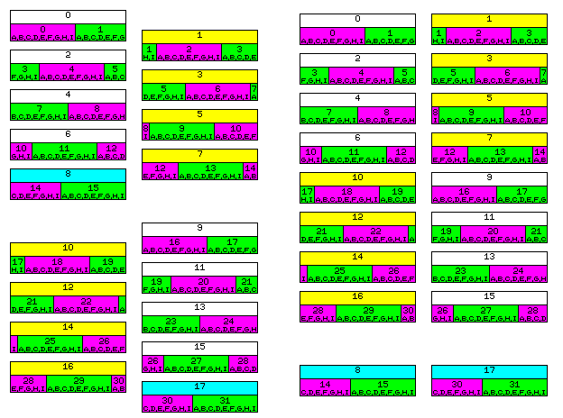
As shown in the diagram, one important difference is that the larger area of memory now includes contiguous 128-bit blocks of memory from both data buses.
If it were desired to create an extent of memory with an apparent 60-bit word length, since 15 is 1111 in binary, one would have to allocate four areas of memory, with sizes in the ratios of 8, 4, 2, and 1.
This scheme can lead to a setup which can even use standard components, and fully provide all the flexibility that is desired, as shown in the diagram on the left.
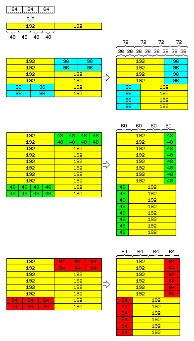
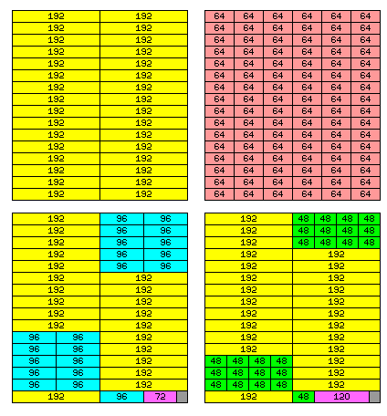
Let us design our microprocessor so that it uses dual-channel memory, with each channel being 192 bits wide. Then, the memory in each channel is composed of three standard 64-bit sticks of DRAM.
This memory, as it is, supports the 48-bit word as its fundamental data type. All the multiples of 12 bits could, of course, be accessed within that memory organization, with allowance for unaligned operands, which having dual channel memory grants.
But in addition:
If we divide the width of the memory on one channel into half, so as to supplement the memory on the other channel with an extension of half its width, then one creates memory that is one and one-half times as wide, so instead of supporting 24, 48, and 96 bits, one could allocate blocks of memory to be used to support 36 and 72 bits.
In this memory organization, 36-bit floating-point numbers could always be kept in strict alignment.
The left side of the diagram shows the actual physical organization of memory, and the right side shows the logical organization which simple circuitry in the processor causes memory to appear to have to programs.
And if we divide the width of the memory on one channel into quarters instead, now we can make memory that is one and one-quarter times as wide, thus allowing 60-bit floating-point numbers to always be strictly aligned.
Finally, we come to a case that will require having a fast divide-by-three circuit; fortunately, we have seen that this is possible.
By dividing one memory channel into three parts, we are able to allocate blocks of memory that are organized in the conventional manner, around the unit of 64 bits, thus permitting compatibility with ordinary computers in addition to the flexibility to fully support the desired ideal floating-point sizes, and emulation of many older architectures.
But one important factor comes to mind which has not been accounted for in the discussion above.
Main memory in a typical modern computer is composed of DRAM modules, not core or even static RAM.
One characteristic of modern DRAM modules is that they are most efficiently accessed when sixteen consecutive locations are accessed in rapid succession - and those sixteen locations can't just be any sixteen locations, but must be aligned on addresses that are multiples of sixteenk times the size of a line of memory.
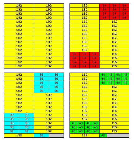
Using a 384-bit wide dual-channel memory to provide flexibility along the lines of the scheme given above, for two lengths, as shown in the top half of the diagram at left, there is no problem.
If one is accessing memory according to a 48-bit word, then no special steps have to be taken to see memory as other than what it actually is, so we just have a unit of sixteen consecutive 384-bit memory lines, as seen in the upper left corner.
If one is accessing memory according to a 64-bit word, then we are taking the 192-bit memory line in one channel, and seeking to organize it in units of 1 1/3 such memory lines. As that is 4/3, and sixteen is a multiple of four, we can perform the reorganization on blocks of sixteen memory lines, as shown in the upper right.
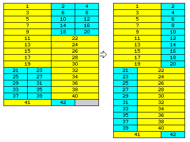
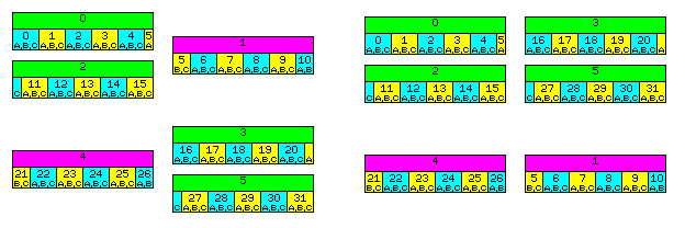
On the right, to make it clear how this scheme is intended to work, the portions of each memory line are numbered serially in the order in which they appear in the logical view of memory, on the right, and are shown on the left in the physical view, with each area being given the same number. Only the case of the 36-bit memory word is illustrated in this way, as it should be trivially apparent what the ordering of the other cases would be on the same principles.
For 36-bit and 60-bit memory words, though, we are using units of 1 1/2 and 1 1/4 memory lines. That means 3/2 and 5/4, and sixteen is neither a multiple of three nor a multiple of five.
However, three times five is fifteen, which is only one less than sixteen.
So, as shown in the bottom half of the diagram, we perform the reorganization of memory on a block of fifteen memory lines, and then only use what we can, either the first 288 bits, for eight 36-bit words, or the first 240 bits, for four 60-bit words, of the sixteenth memory line in a block.
So we are able to make full use of memory bandwidth when reading memory normally, rather than two-thirds, three-quarters, or five-eighths of memory bandwidth, as would be the case when reading a single memory line at a time, but we are required to waste 1/64th of memory when using the 36-bit word, and 3/128ths of memory when using the 60-bit word.
However, while the consequences are beneficial as regards memory bandwidth, there is another important consequence of this memory organization.
As before, in the case of a 48-bit memory word, physical addresses correspond directly to logical addresses, and in the case of a 64-bit memory word, physical addresses require a divide-by-three circuit to be generated from logical addresses.
However, previously, in the cases of the 36-bit and 60-bit memory words, physical addresses could be generated from logical addresses using simple multiplications requiring a shift and an add. Now, division circuits are instead required.
In the case of the 36-bit word, a divide-by-21 circuit is required. This
can be achieved by the use of a divide-by-three circuit and a divide-by-seven
circuit, and as three is 11 in binary, and seven is 111
in binary, the simple end-around-carry design for the division circuit previously
examined is possible.
In the case of the 60-bit word, however, a divide-by-25 circuit is required.
However, since fifteen, a multiple of five, is 1111 in binary, again
the end-around-carry design for the two division circuits to be cascaded is again
available.
The reason that the 48-bit word had to be chosen as the fundamental word length for this design, rather than the 36-bit word length or the 60-bit word length, is because in addition to the base case, where the full contents of two data buses are fetched at once and used directly, all the other cases provided have to involve a logical view in which data is organized as 1 + (1/n) times the width of a data bus, for some positive integer n.
So, with a 48-bit word as the basis, a 40-bit word can't be supported directly using this method. That's because, given a data bus of 192 bits in width, 320 bits is equal to 1 2/3 times 192 bits.
So a single fetch from physical memory would provide 192 bits of data on one data bus, and, to make up the desired 320 bits of data, 128 bits on the other data bus. But then the 64 bits which aren't used can't be used as part of the next 320 bit logical memory line in a single fetch; at least 128 bits must be available to combine with 192 bits to make another 320 bits.
However, a workaround is present. If memory is organized as it would be for the 60-bit word size, then logical memory lines of 240 bits in width are fetched from memory. 240 bits is a multiple of 80 bits as well as 40 bits, allowing aligned 80-bit data to be handled efficiently; all that is needed is to add an additional divide-by-three circuit to the scheme of memory addressing for the 60-bit word to allow 40-bit operation to be handled.
Another consideration is that, since the native 384-bit memory line is a multiple of 64 bits (and 128 bits), instead of using the technique described here to form memory lines of 256 bits from 1 1/3 half lines, it is also possible to support memory based on the 64-bit word more simply, by using a divide-by-three circuit for addressing.
As this is much simpler, it likely should be the preferred technique, leaving the butterfly scheme for the 36-bit and 60-bit word lengths.
Finally, while only a small amount of memory is left unused in the cases of the 36-bit and 60-bit words, there may be room for improvement available.
In the case of the 36-bit word, the last 96 bits in each block is left unused.
If there is no need for aligned 144-bit units of memory, with 72 bits being the length of the widest data type, then the first 72 bits of those final 96 bits could also be used.
In that case, instead of a divide-by-21 circuit being required to convert logical addresses into physical addresses, there being 21 logical memory lines of 288 bits in a physical block of 16 physical memory lines of 384 bits, now there would be 85 doublewords of 72 bits in 16 physical memory lines of 384 bits.
85 is equal to 5 times 17. 5 times 3 is 15, which is 1111 in binary, and 17 times 15 is 11111111 in binary, so such a fast division circuit is realizable. In fact, it's realizable in one stage, since 85 times 3 is 255, with 255 being 11111111 in binary, so one multiplies by three and divides by 255 in the usual fashion.
In the case of the 60-bit word, the last 144 bits in each block is left unused.
If no aligned unit of memory larger than 120 bits is required, then the first 120 bits of those final 144 bits could also be used.
Now, instead of there being 25 logical lines of 240 bits in a physical block of 16 physical memory lines of 384 bits, there would be 51 units of 120 bits in 16 physical memory lines of 384 bits.
51 is equal to 3 times 17; 3 is 11 in binary, and as has already been mentioned, 17 times 15 is 11111111 in binary, and so, once again, the required division circuit is realizable. And again in one stage, as 51 times 5 is 255.
The diagram to the right shows how memory would be organized for the 48-bit, 64-bit, 36-bit and 60-bit widths with the modifications described here. Note that now in both the 36-bit and 60-bit cases, only the last 24 bits of each block are left unused.
Also, note that these diagrams are based on realizing the memory with the use of DDR4 memory modules. Since DDR5 memory modules each contain two channels of memory that are 32 bits in wide, using DDR5 modules in sets of three to allow for a memory bus half as wide to be organized in this basic fashion for the same flexibility in word lengths is possible.