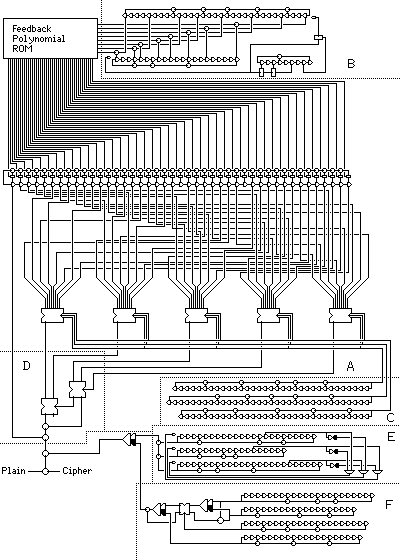
The following diagram:
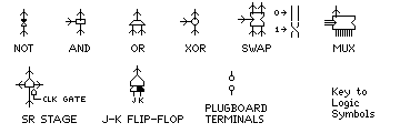
Symbols used:
illustrates various ways in which shift registers can be used to produce pseudorandom bits, combining them in an elaborate construction.
The device is based primarily on the Kinetic Protection Device, a stream cipher device produced by a defense contractor which has been openly described. But I have modified it significantly; in some ways to improve security, in others to reduce the number of components to fit into a reasonably sized diagram. And I have added sections illustrating other stream cipher principles, one based on a claimed cellular telephone cipher algorithm.
The output bitstream of the main portion of the device is XORed to a bitstream produced by a combination of two different constructs.
The first of these, illustrated in section E of the diagram, is based mainly on the A5 cellular telephone algorithm, but made simpler to draw by replacing its self-clocking principle by that of the T-52. The second, in section F illustrates the use of J-K flip-flops to combine shift registers nonlinearly.
The Kinetic Protection Device generated an 8-bit output each time the shift register in it was clocked. A shift register of 61 stages was used, and the feedback polynomial applied was selected from a set of 1024 such polynomials stored in ROM. Eight different nonlinear functions, each taking six bits of input from six stages of the shift register, were used to produce the eight bits of output.
The design pictured here uses a 44 stage shift register, with a ROM having only 256 feedback polynomials in it. The main part of this circuit is section A of the diagram. The modified Geffe generator, here found in section D, shown earlier on this page in ASCII graphics, takes five inputs from five stages of the shift register; the newest bit in the shift register is then XORed to the result. While there is only one nonlinear function, the five inputs to the modified Geffe generator can each be chosen from eight sources in the shift register, and this is determined by bits from three other shift registers in section C. The output of these three shift registers is XORed with signals produced in other parts of the device for some extra difficulty in analyzing its output. Thus, the design produces only one bit of output, not eight bits, each time the shift registers in it are stepped.
Instead of the feedback polynomial of the main shift register being set once as part of the key, it varies during encipherment. The eight-bit input to the feedback polynomial ROM is produced by selected bits from two shift registers moving in opposite directions, XORed together in section B. These shift registers are clocked by the AND of three bits from a third shift register, so that the feedback polynomial only changes at intervals. Since all the feedback polynomials in the ROM are maximal period ones, as long as the initial state of the LFSR stages is nonzero, it will remain nonzero.
That arrangement does have the weakness that all eight output bits are parts of the same sequence of bits, although at widely separated intervals: the bits produced by XORing the output of the two shift registers with different periods. (That may not be strictly true if the periods of the two generators is not relatively prime.) This weakness is reduced by using the OR of two other bits of the clocking shift register to AND one of the clock signals, so that the two main shift registers will not be perfectly in step. The result is, however, still the same sequence of bits being produced on each line, but a different sequence with a longer period is appearing there, at least. This shows the merit of the original Kinetic Protection Device design, since, unlike my efforts here, it does avoid that; however, this circuit is at an earlier position. Thus, we can choose to stop at any point, as otherwise we get infinite regress, or what one book on computer graphic displays has called the "wheel of reincarnation".
This output is XORed with the output of a J-K flip-flop, which has as inputs the bitstreams produced in sections E and F of the diagram. A J-K flip-flop is a good way to combine two bitstreams for reasons which are explained below, in the description of the section of the device which illustrates their use.
The first bitstream used is produced by three shift registers which clock each other, in section E of the diagram. Each one is clocked by the OR of two bits (one inverted) from each of the other two shift registers. Since each shift register supplies one bit and the negation of that same bit to the clocks of the two other shift registers, it is never possible for all three shift registers to stop moving at the same time. Just as the main part of the schematic is inspired by the Kinetic Protection Device, this part is inspired by the A5 algorithm used with GSM cellular telephones.
The second bitstream comes from a circuit which includes one element that is very likely to have been part of the electronic cipher machines of the early 1970s, the J-K flip-flop. This is section F of the diagram. In the book Basic Methods of Cryptography, by Jan C. A. van der Lubbe is noted something I really should have recalled from learning about digital circuitry as an undergraduate: a J-K flip-flop, in addition to being set if a signal is sent on J alone when it is clocked, or being reset by K alone, is unaffected if neither is present, and is toggled when both are present. This makes it as unbiased as an XOR for combining two bitstreams, but its memory makes it nicely nonlinear.
The circuit supplying the second bitstream consists of four shift registers. Two of them are used as inputs to both a J-K flip-flop and an XOR gate. Then, the two output bitstreams resulting are selected by the output of a third shift register. One is used as an input to another J-K flip-flop, along with the output of a fourth shift register, and the other output bitstream resulting from the first two shift registers is XORed with the result.
The following table, showing for two inputs the outputs of a J-K flip-flop and an XOR gate,
   J    K     J-K flip-flop   J xor K
 --------------------------------------
   0    0  |        P       |    0
   0    1  |        0       |    1
   1    0  |        1       |    1
   1    1  |       ~P       |    0
illustrates the property of the J-K flip-flop used here: not only is its output a random stream if it has two random streams as input, but this output is uncorrelated with the output of an XOR gate with the same two inputs. So, having a third input choose between the two modes of combining the first two inputs produces an output hard to relate to the raw outputs of any of the shift registers involved. The circuit used in section F of the diagram, as we have seen, begins by using that principle.
In addition to the bits initially loaded into the shift registers of the device, another possible keying element for such a device is the order in which the shift registers of different lengths are connected to the different areas which take input from a shift register. Only those shift registers that are used in a plain fashion, with no values taken from within the shift register and with no special clocking are shown as being switchable via plugboard terminals. In practice, a plugboard would not be used; some circuit with switches would be used instead. The idea of continuously varying the connections with a rotor machine hardly bears thinking about.
Note that I have generally neglected to show the clock pulses explicitly; essentially, all the J-K flip flops and shift register stages are clocked by one master clock pulse, with the exceptions of the shift register gating the clock for the two shift registers used to address the feedback polynomial ROM, and of an implicit 1/2 clock pulse delay for the signals by which the three shift registers in section E of the diagram clock each other.
Also, the reason for my use of nonstandard logic symbols here and in other diagrams is to provide legibility in a small number of pixels (the standard symbols for AND and OR, for example, look alike).
Next
Chapter Start
Skip to Next Chapter
Table of Contents
Main Page