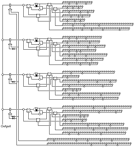
One construction suggested for making use of the properties of the J-K flip-flop is due to Pless: four pairs of shift registers feed into four J-K flip-flops, and their outputs are used in rotation. This eliminates direct information about the raw shift register sequences, which can be obtained from two consecutive bits of their output some of the time.
While attacks on that device have been shown to exist, in practice it would be elaborated upon, and as a starting point it is not a bad idea. The following diagram:
illustrates a possible elaboration. Instead of four groups of two shift registers, we have four groups of seven shift registers. Five are grouped in the fashion we saw in the green-background area of the large diagram above; two feed both a J-K flip-flop and an XOR gate, and these two outputs, together with the outputs of three other shift registers, are applied to the extended Geffe generator circuit described earlier. Two additional shift registers are used to control swapping of the outputs from two pairs of shift registers.
Instead of using the outputs of the four segments in sequence, two shift registers select a segment at random; and that segment is omitted, the outputs of the other three being XORed to produce the final result.
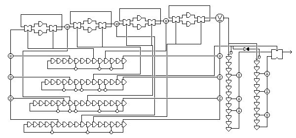
An interesting, secure, and simple shift-register based design is illustrated within the High-bandwidth Digital Content Protection System specification developed by Intel:
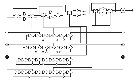
The XOR of the outputs of four shift registers generate a sequence of bits with a long period. The XOR of four other taps, one from each shift register, produce another part of that sequence of bits: since these taps are not all at the same distance from the outputs, that XOR produces a distant part of the same sequence.
Another set of four taps from these shift registers controls four switchable delay or memory cells: each cell stores two previous inputs, and the control signal determines which of those two values is output. The new input replaces the value output, but the two values remaining are then also swapped.
Since what this does is buffer the sequence of bits from the four earlier taps, allowing them to be output after an irregular number of cycles, it is similar to what the MacLaren-Marsaglia random number generator does. Each bit input to these four cells can take many different numbers of cycles before being output, and so there is no one sequence of bits similar to those of a shift register which is particularly likely to match the actual output.
However, it is still true that there is an average amount of time that the bits from the delayed sequence will take to go through the four delay cells, and so it has been claimed that this might be sufficient to provide for a correlation attack, such as that used against the Geffe generator.
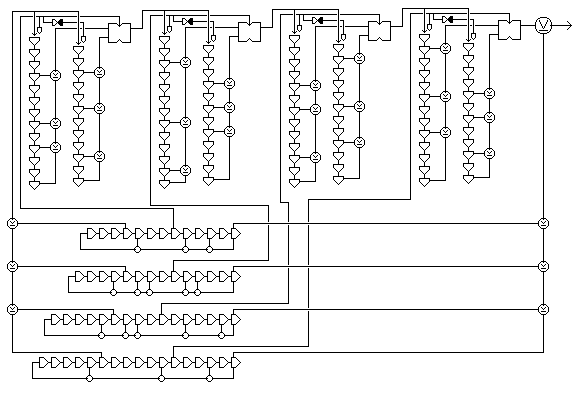
The following diagram:
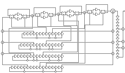
indicates two simple ways in which this design can be improved to make it considerably more resistant to such an attack.
The first change is that between each pair of delay cells, another output from the shift registers is XORed with the bits as they progress. This means that different cases of individual amounts of delay in the four cells which add up to the same total delay are no longer equivalent.
The second change is that another shift register is used to store several successive outputs from this generator, and the actual output used is the XOR of four of these outputs. Now, a bit of output will belong to the 'most likely' case sought by a correlation attack only if the four output bits of the previous part of the generator all belong to that case.
However, that last bit of the generator, while it does prevent a direct correlation attack, doesn't really add any security, since the input to that stage can be derived from its output by a very simple process of deconvolution. So it is not enough to use multiple bits of the output, they must be chosen unpredictably. A valid design using this principle might look like this:
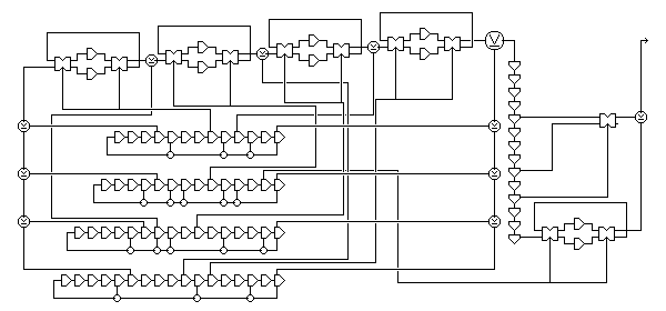
where three of the old bits are combined by a nonlinear function, and the other one goes through another variable delay cell. Now, an actual, although modest, gain in security against a correlation attack is obtained.
However, a simple idea allows the very large gain in security against a correlation attack aimed at by the first of the extended versions of this design to be achieved. In the following diagram:
the outputs of the main generator are directed alternately to one of two shift registers. The one that recieves the output is the one that is stepped, and the one from which the XOR of four bits is used. In this way, the four outputs of the main generator which are used vary over a large number of possibilities.
Since the decorrelator circuit added at the end of the device seems to be so powerful, perhaps we could go back to taking only the original number of taps from the shift registers:
but replace the variable delay cells of the original design with decorrelator circuits. In this way, the final output is formed from any of a huge number of possible combinations of the shift register outputs.
Incidentally, it may have occurred to you from viewing the diagrams above that a decorrelator circuit could as easily be built using the principle of selective recycling used in the delay cells in the original design, as shown here:
as by using the principle of selective clocking. The XOR of other bits besides the one clocked out could even include bits from the shift register row not used, as well.
Hence, even if the design shown is not considered perfect, minor changes can strengthen it considerably.
Next
Chapter Start
Skip to Next Chapter
Table of Contents
Main Page